Advanced RF technologies
Imec’s Advanced RF program explores the next generation of wireless networking. Our approach combines the benefits of silicon CMOS and III-V technologies, based on concrete system needs.

Connectivity is more crucial than ever. As 5G rolls out, the industry already looks ahead to meet demands for faster data rates, lower energy consumption, and reduced latency.
By expanding the frequency spectrum above 6 GHz, larger bandwidths become available. The FR3 (Frequency Range 3) spectrum, ranging from 7-24 GHz, is gaining interest for its potential to balance capacity and coverage effectively.
Looking further, 6G will move to even higher frequencies: mmWave bands well above 100 GHz. This will enable new use cases that thrive on networks of diverse devices and new modes of human-machine interaction, such as:
- Capturing and delivering true mixed reality (XR) that merges real and virtual worlds.
- Exchanging large amounts of data for federated learning between AI systems, like in autonomous cars.
III-V Devices for Beyond 5G and 6G
These higher frequencies bring quite some challenges. The most important one being that silicon CMOS can no longer efficiently deliver the necessary performance, especially in critical front-end module (FEM) components like power amplifiers.
The solution comes from III-V semiconductors such as gallium nitride (GaN) and indium phosphide (InP). Their material properties enable them to outperform silicon CMOS, providing the required output power and efficiency at high operating frequencies.

Imec’s Advanced RF program paves the way for high-performance, energy-efficient, scalable, and low-cost radio solutions by integrating GaN and InP into established CMOS processes. Our R&D spans two levels:
- Device challenges: Bringing GaN and InP devices to 200- and 300mm silicon wafers, requiring novel manufacturing techniques, new system and circuit design approaches, etc.
- System challenges: co-integrating these GaN-on-Si- and InP-on-Si-based components, used for power amplifiers and possibly low-noise amplifiers and switches, with CMOS components for functions like frequency synthesis, up- and down-conversion, calibration, control, and beamforming.
RF GaN-on-Si for beyond 5G
Unlike GaN-on-SiC, currently used for some high-frequency RF applications, GaN-on-Si is suitable for mass production on 200- or 300mm wafers. Imec leverages its experience with Gan-on-Si for power devices and optimizes this platform for RF use.
Longread: DC Reliability of high-κ GaN-on-Si MOS-HEMTs for mmWave power amplifiers
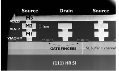
Some features of imec’s RF Gan-on-Si technology:
- CMOS-compatible 200mm RF GaN-on-Si process
- In-house MOCVD growth of RF buffer and active layers (AlGaN, InAlN)
- HEMT and MISHEMT devices with Lg < 50nm and low resistive Ohmic contacts with Rc <0.15 Ω mm
- Advanced multi-layer Cu BEOL & integration of passives
Our offering includes:
- Device design and optimization to meet the performance and reliability requirements for Beyond-5G infrastructure and handset applications.
- Modeling and advanced characterization for technology pathfinding, including reliability and thermal design.
- Exploration of novel device architectures and engineered substrates.
- RF GaN-Si R&D design platform for circuit exploration and technology customization.
- FEM system and circuit design, including system-technology co-optimization and benchmarking with incumbent technologies.
- Demonstrators displaying the advantages of RF GaN-on-Si.
RF InP-on-Si for 6G
For frequencies around and above 100 GHz, InP offers the best power-efficiency trade-off. However, its potential is limited as long as its fabrication depends on lab processes on small wafers.
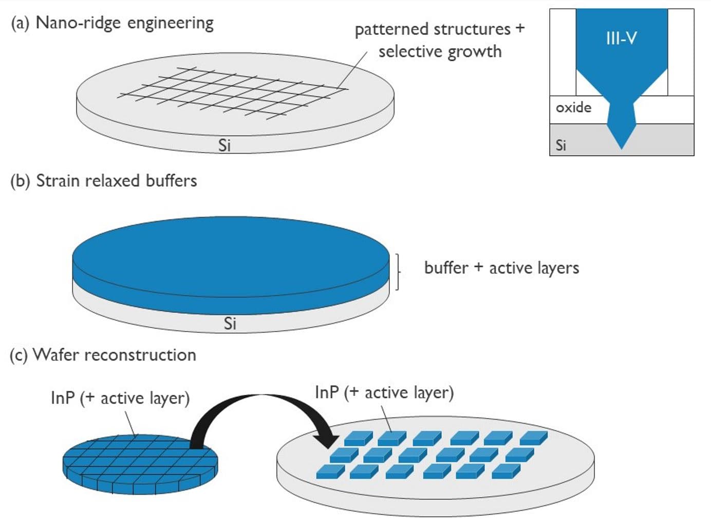
Imec aims to make InP manufacturing processes CMOS-compatible. Three approaches are considered for integrating InP on silicon:
- Nano-ridge engineering: Selectively growing III/V material in pre-patterned trenches in silicon.
- Strain-relaxed buffers: Growing InP on layers deposited on silicon to compensate for the lattice mismatch between Si and InP.
- Wafer reconstruction: Using die-to-wafer bonding to attach tiles made from high-quality InP substrates to a silicon wafer.
Dive into this article for more details
RF silicon interposer for heterogeneous integration of III-V with CMOS
Once the manufacturing of III-V devices is scaled up, further cost reduction is possible by limiting the use of these costly devices to areas where their performance is essential. Other parts of the system can then still be developed in silicon CMOS.
This chiplet approach stems from imec’s expertise in 3D integration. Technologies like scaled micro-bumps, high-aspect-ratio through-silicon vias (TSVs) and multi-layer Cu damascene routing enable heterogeneous integration through Si interposer technology, offering a smaller footprint and lower loss compared to advanced PCB technology.
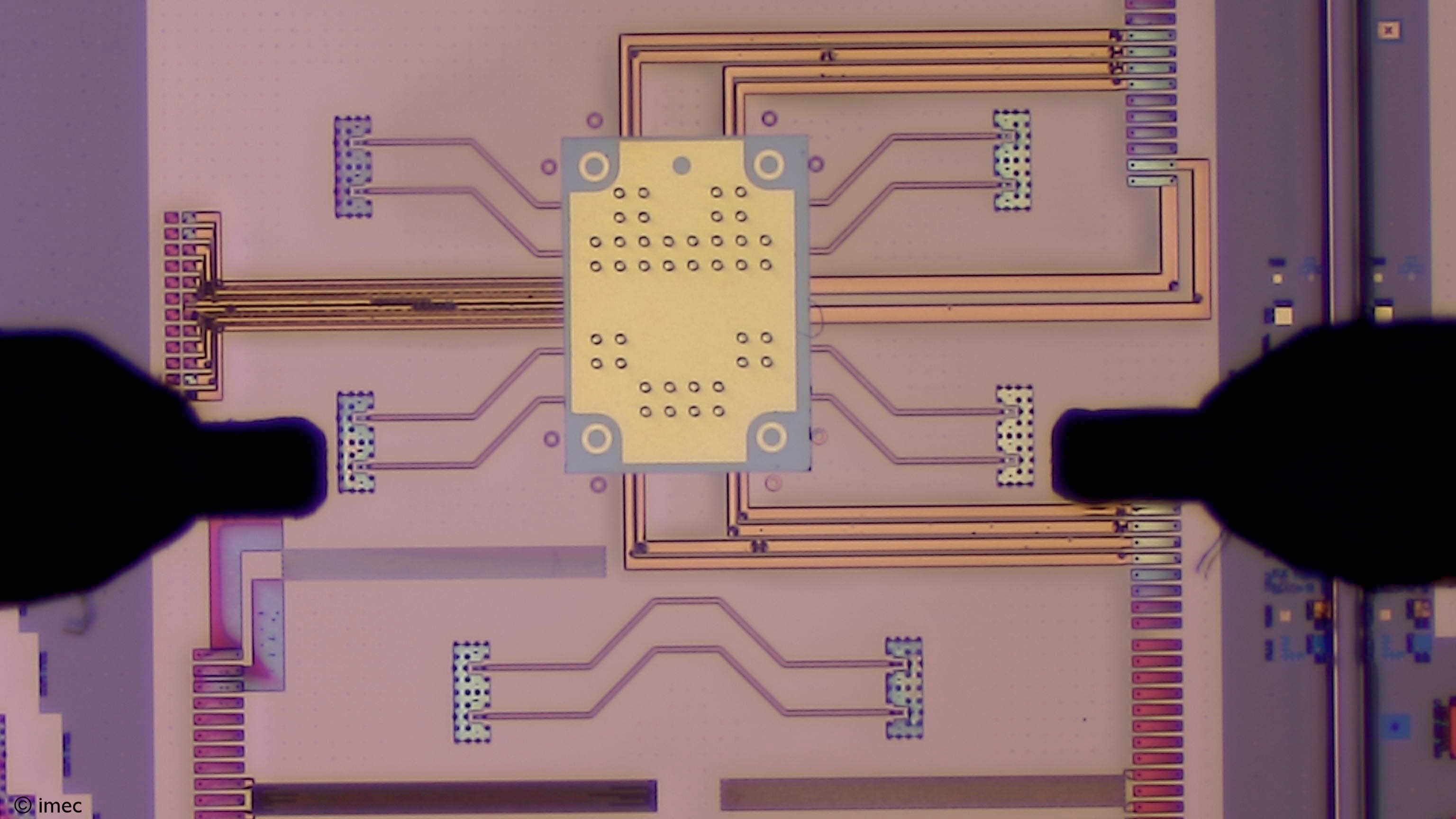
Some features of imec’s RF interposer technology:
- Through-silicon vias (TSVs)
- High-density digital interconnects
- Thick RF polymer processing
- Multi-layer redistribution layers
- High-Q passives including resistors, inductors, MIM capacitors
- Micro-bumping to Cu & Au BEOL of ICs
- Improved thermal conductivity
- 300mm fab compatible
Our offering includes:
- RF Si interposer R&D developing new features (passives, TSV integration, wafer thinning, etc.) and exploring new materials.
- System-technology co-optimization (STCO) for achieving optimal radio functionality partitioning and guiding device process technologies and packaging/interconnection approaches.
- Modeling and advanced characterization for technology pathfinding, including reliability and thermal design.
- RF interposer R&D platform for prototyping and technology customization.
Download leaflet for more details
Want to partner with imec on beyond 5G and 6G?
- Join the program to get early access to imec’s R&D results. Co-develop the next RF technologies through precompetitive, cost- and risk-shared research.
- Enter into a bilateral development project to leverage imec’s technology and expertise to realize a prototype or technology demonstrator for your specific requirements.
Beyond 5G technology blogs
"It’s time to start imagining the kind of 6G we want"
Imec fellow Piet Wambacq shares his vision on where the next generation of cellular connectivity can take us. And on what we need to realize that future.
"To reap the rewards of 6G, we need to start sowing the seeds now"
Michael Peeters, VP R&D connectivity at imec, explains why there is no time like the present to tackle some key technologies that will make or break 6G.
"To boost 6G energy efficiency, we need models that can handle its complexities"
Margot Deruyck, FWO-Postdoctoral Fellow at WAVES, an imec research group at Ghent University, dives into the power consumption of next-gen wireless networks.
Presentations, articles and press releases on beyond 5G technology
- Imec introduces best-in-class ADCs, propelling beyond-5G communications
- Imec unveils CMOS-based 56Gb/s zero-IF D-band beamforming transmitter, featuring superior output power and energy efficiency
- EuCNC & 6G 2021 Summit keynote by Michael Peeters
- Future Scaling: Where Systems and Technology Meet, presented by Nadine Collaert at ISSCC2020
- IMS 2019 keynote by Michael Peeters
- New imec research program pursues the development of scalable and energy-efficient 6G device technology
- Heterogeneous III-V/CMOS technologies for beyond-G RF front-end modules
- Imec demonstrates scalable III-V and III-N devices on Si targeting beyond 5G RF front-end modules
- Heterogeneous integration technologies to enable the next generation of wireless 6G
- Scaling up GaN- and InP-based technologies for 5G and 6G wireless communication
- Imec demonstrates GaN-on-Si MISHEMTs with excellent performance for 5G-advanced base station and mobile device applications
- Imec achieves seamless InP Chiplet integration on 300mm RF Silicon Interposer with excellent performance at 140GHz
- DC Reliability of high-κ GaN-on-Si MOS-HEMTs for mm-Wave Power Amplifiers
- Imec identifies stable operating range for GaN MISHEMTs in RF power amplifiers
- 300mm RF silicon interposer platform for chiplet-based heterogeneous integration demonstrates record-low insertion loss at frequencies up to 325GHz
- Imec achieves record-breaking RF GaN-on-Si transistor performance for high-efficiency 6G power amplifiers
Scientific publications
Tang et al. “A 140 GHz T/R Front-End Module in 22 nm FD-SOI CMOS”, IEEE Radio Frequency Integrated Circuits Symposium (RFIC), (2021)
External linkParvais et al. “GaN-on-Si mm-wave RF Devices Integrated in a 200mm CMOS Compatible 3-Level Cu BEOL”, IEEE International Electron Devices Meeting (IEDM), (2020)
External linkVais et al. “First demonstration of III-V HBTs on 300 mm Si substrates using nano-ridge engineering”, IEEE International Electron Devices Meeting (IEDM), (2019)
External linkPhD and postdoc opportunities for beyond 5G technology
Do you (almost) have a master’s degree in electrical engineering, computer science, or another related field? Are you excited about the recent evolutions in beyond 5G? And do you want to help change the world by making communication ubiquitous, sustainable intelligent and/or invisible? Then you should consider applying for a PhD or postdoc position at imec.
Read more

Imec unlocks system-level III-V chiplet integration on Si-CMOS by advancing its 300mm RF silicon interposer platform with high-density MIMCAPs, passive modeling, and laser-assisted bonding
Read more
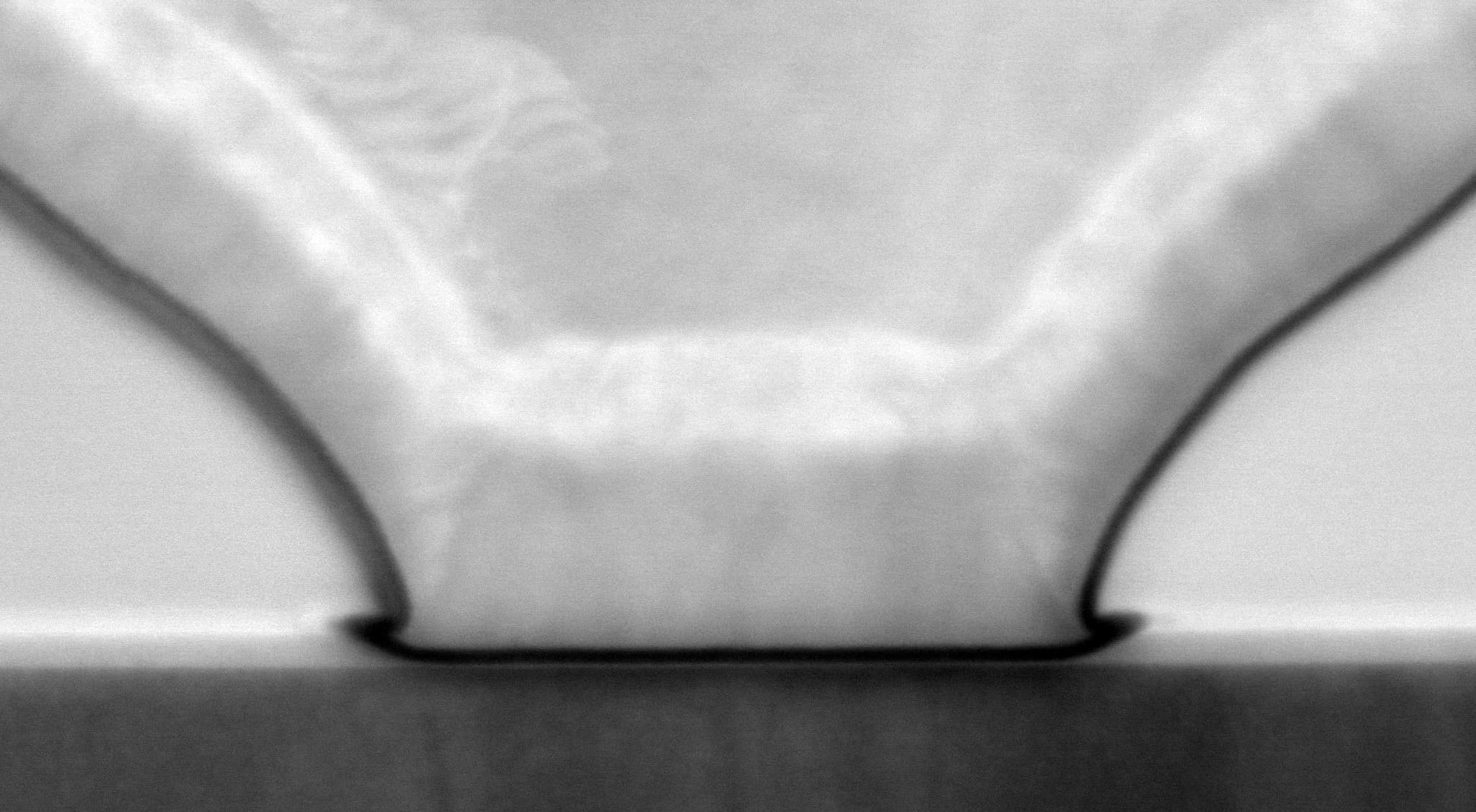
Imec achieves record-breaking RF GaN-on-Si transistor performance for high-efficiency 6G power amplifiers
Improved contact resistance and RF output key toward mobile-compatible E-mode GaN-on-Si transistors
Read more
ITF USA 2026 at SEMICON® West
From silicon to systems: building the AI future The pace of AI evolution leaves little room for certainty. Yet, several trends are clear: AI agents increasingly collaborating in orchestrated ecosystems are on the rise. Physical AI is a crucial next step, including (humanoid) robots transforming our homes and workspaces. In parallel, AI – just like advances in quantum computing – could help unlock breakthroughs in fields such as physics and biology. Building the AI future starts with a solid hardware foundation – from high-performance, energy-efficient compute in the data centers to low-power, real-time inference at the edge. ITF USA at SEMICON® West presents the building blocks for shaping the AI future. On October 12 in San Francisco, we take stock of the full AI deep-tech stack: from silicon to systems, from research to manufacturing. Discover ITF USA
View event