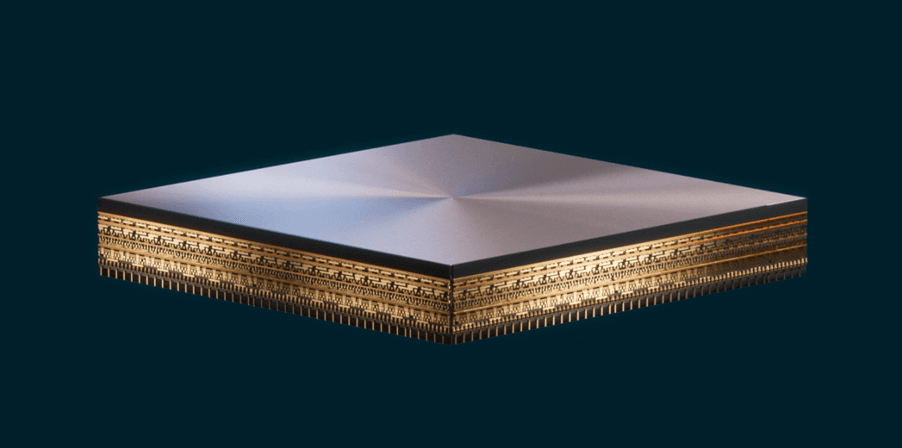
Scaling up GaN- and InP-based technologies for 5G and 6G wireless communication
GaN HEMTs and InP HBTs: integration on a Si platform and co-integration with CMOS components
In short
With the advent of next generation 5G and 6G, telecom operators are pushing up the frequencies of the wireless signals.
While GaN high-electron mobility transistors (HEMTs) show promises for 28/39GHz operation, InP heterojunction bipolar transistors (HBTs) are expected to excel at 100GHz and beyond.
In this article, progress is reported in upscaling GaN HEMTs to a silicon platform and in co-integrating them with CMOS components – requirements for next-gen high-capacity wireless communication. Also discussed is the exploration of InP for 6G.
Year after year, more and more data are being transmitted wirelessly by an ever-growing group of users. To keep up with this trend and make data transfer faster and more efficiently, the fifth generation (5G) of mobile communication is being rolled out, and the industry is already looking at what lies beyond. While 5G enables peak data rates of 10Gbit/s, 6G is projected to operate at 100Gbit/s from 2030 onwards. In addition to coping with more data and connections, researchers investigate how the next generation of wireless communication can support new use cases such as autonomous driving and holographic presence, among others.
To enable these exceedingly high data rates, the telecom industry has been pushing up the frequencies of wireless signals. While 5G initially uses sub-6GHz frequency bands, products targeting 28/39GHz are already showcased. Additionally, there is a growing interest in using FR3 (6-20GHz) frequency bands for 5G networks due to their ability to balance coverage and capacity. For 6G, frequencies above 100GHz are being discussed.
Moving toward higher frequencies has several advantages: new frequency bands can be used, solving the spectrum scarcity issue within existing bands. Also, the higher the operating frequency, the easier it is to obtain wider bandwidths. Frequencies above 100GHz and bandwidths up to 30GHz allow telecom operators, in principle, to use lower-order modulation schemes within the wireless data links, which reduces power consumption. Higher frequencies are also associated with smaller wavelengths (λ). As the antenna array size scales with λ2, antenna arrays can be packed more densely. This contributes to better beamforming, a technique that ensures that a larger fraction of transmitted energy reaches the intended receiver.
But the advent of higher frequencies comes at a price. Today, CMOS is the preferred technology for building the critical components of transmitters and receivers. These include the power amplifiers within the front-end modules that send the radio frequency signals to and from the antennas. The higher the operating frequency, the more the CMOS-based power amplifiers struggle to deliver the required output power with sufficiently high efficiency.
And that’s where technologies such as GaN and InP come into play. Due to outstanding material properties, these III/V semiconductors are more likely to provide the required output power and efficiency at high operating frequencies. GaN, for example, has a high current density, high electron mobility, and large breakdown voltage. The high power density also allows for a small form factor and, thus, a reduction in overall system size at the same performance.
GaN and InP outclass CMOS at higher operating frequencies
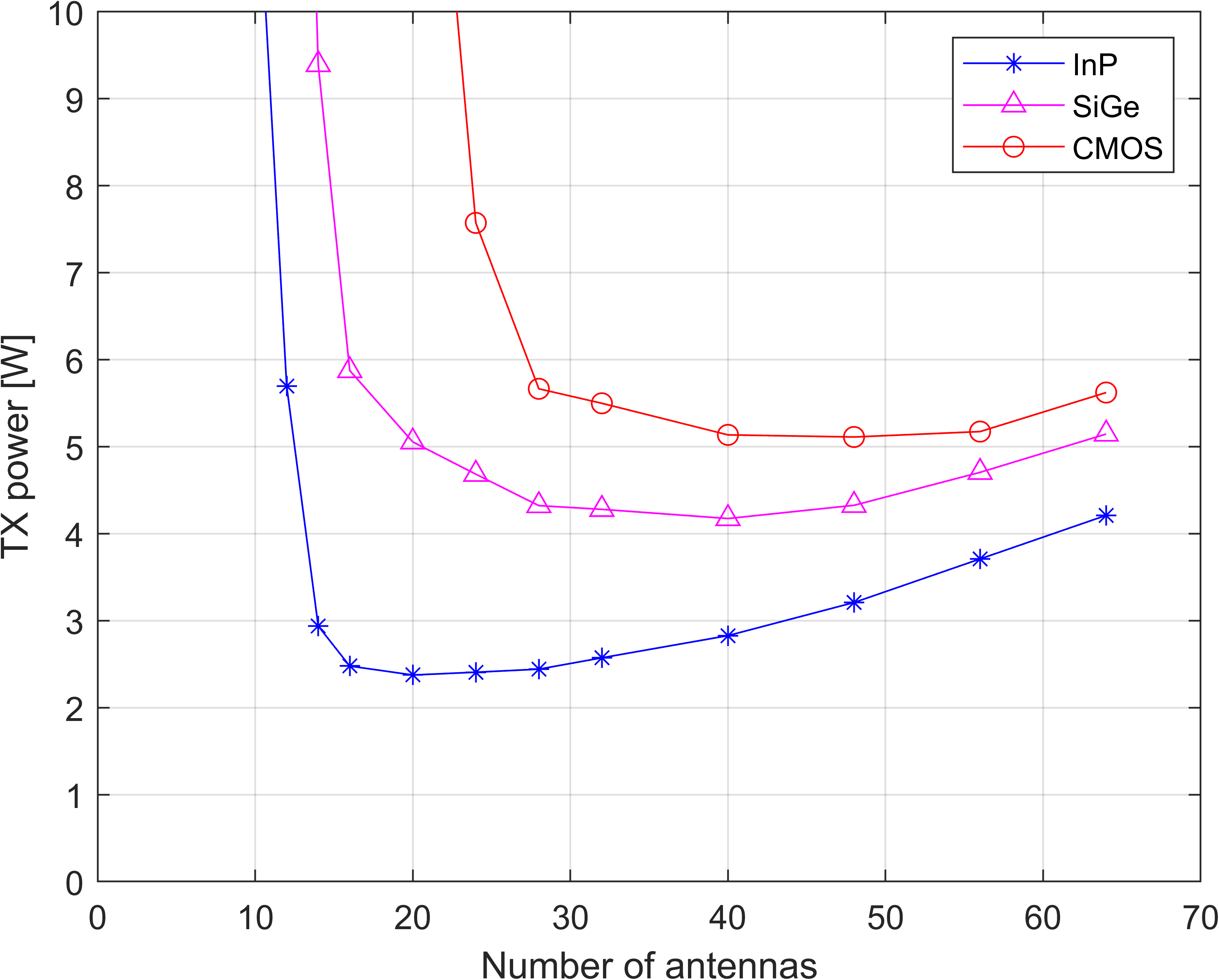
In a modeling exercise, researchers at imec compared the performance of three different power amplifier implementations at 140GHz operating frequency: a full CMOS implementation, a CMOS beamformer with SiGe heterojunction bipolar transistor (HBT), and an InP HBT. InP was the clear winner in terms of output power (over 20dBm) and energy efficiency (20 to 30 percent). Modeling results also indicate that for InP, the optimal point for energy efficiency is obtained with a relatively low number of antennas. This is especially interesting for footprint-restricted use cases like user equipment (e.g., mobile devices).
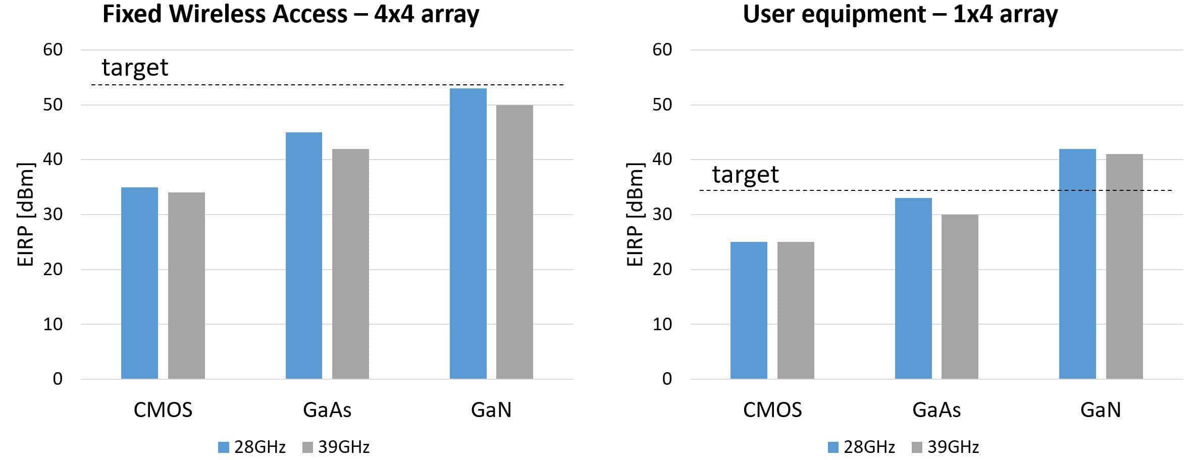
At lower mm-wave frequencies, however, GaN shows excellent performance. For both 28 and 39GHz, high-electron mobility transistors (HEMTs) made of GaN-on-silicon-carbide (GaN-on-SiC) are observed to outclass CMOS-based devices and GaAs HEMTs in terms of output power and energy efficiency. Two different use cases were considered, i.e., fixed wireless access (FWA, with 16 antennas) and user equipment (with four antennas).
Opportunities and challenges for upscaling
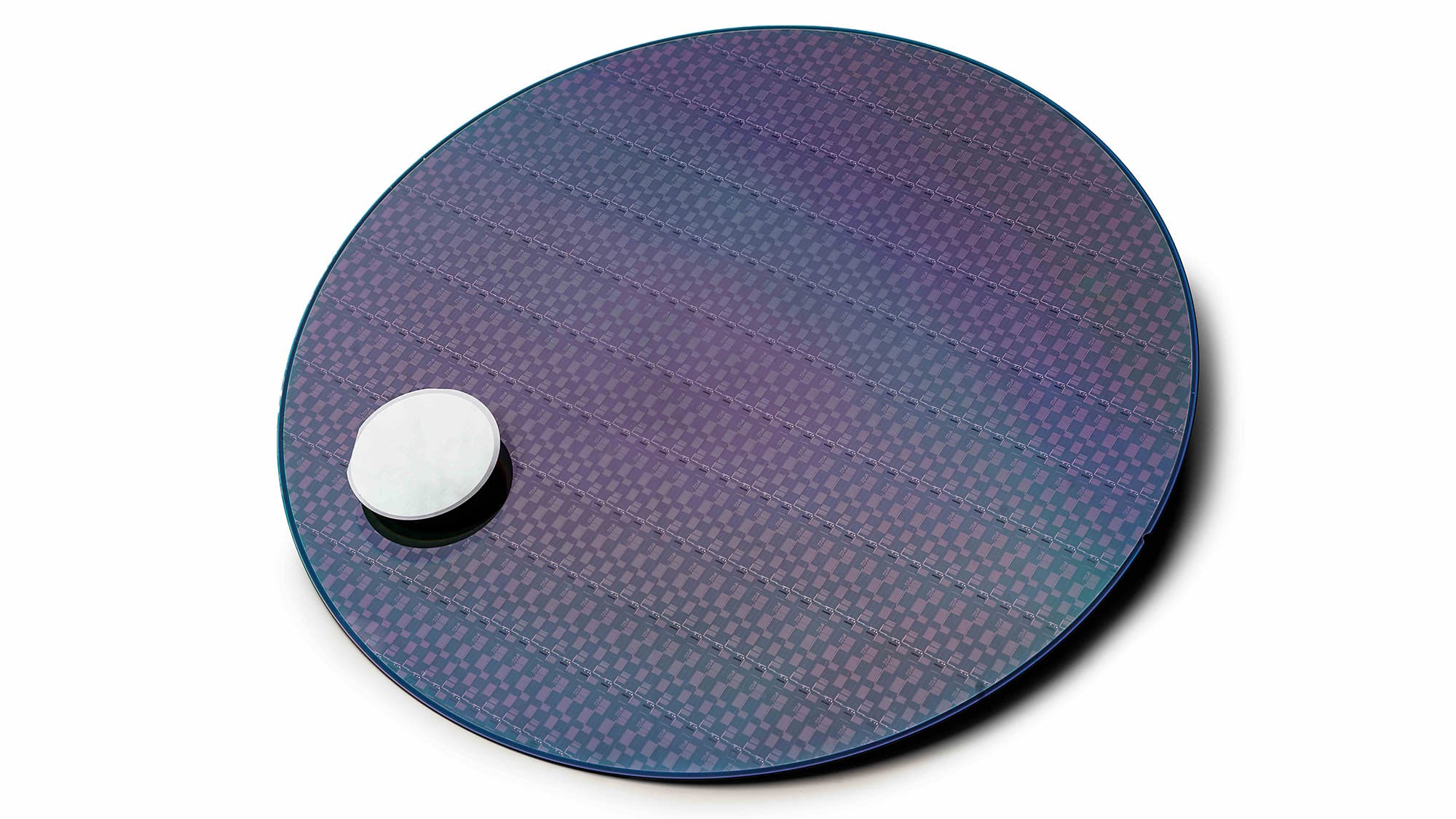
But if we consider cost and ease of integration, GaN and InP device technologies cannot yet fully compete with CMOS-based technologies. The III/V devices are typically made on small and costly non-Si substrates, relying on less suitable processes for high-volume manufacturing. Integrating these devices on 200 or 300mm Si wafers is an interesting approach to achieving overall optimization while maintaining superior RF performance. Not only are Si substrates cheaper, but the CMOS-compatible process also enables large-scale manufacturability.
Integrating GaN and InP on a Si platform requires a combination of new transistor and circuit design approaches, materials, and manufacturing techniques. One of the main challenges relates to the large lattice mismatch: eight percent for InP, and 17 percent for GaN. This is known to create many defects in the layers, which ultimately degrade device performance.
In addition, we will have to co-integrate the GaN-on-Si- and InP-on-Si-based components with CMOS-based components into a complete system. GaN and InP technologies will initially be used to realize the power amplifiers within the front-end modules. Also, low-noise amplifiers and switches could potentially benefit from the unique properties of these compound semiconductors. But in the end, CMOS will still be needed for calibration, control, and beamforming.
Within its Advanced RF Program, imec, with its industry partners, explores various approaches to integrate GaN and InP devices on large-size Si wafers, and how to enable their heterogeneous integration with CMOS components. Pros and cons are being assessed for different use cases – infrastructure (such as FWA) as well as user equipment.
Improving GaN-on-Si technology for RF performance
Depending on the starting substrate, there are several flavors of GaN technology: GaN bulk substrates, GaN-on-SiC, and GaN-on-Si. Today, GaN-on-SiC is widely explored and already used for infrastructure applications, including 5G base stations. GaN-on-SiC is more cost-efficient than bulk GaN technology, and SiC is an excellent thermal conductor – helping to dissipate the generated heat in high-power infrastructure applications. However, the cost and limited size of the substrate make it less suitable for mass production.
GaN-on-Si, on the contrary, has the potential to be upscaled to 200mm and even 300mm wafers. Thanks to years of innovation for power electronics applications, the integration of GaN on large-size Si substrates has made tremendous progress. But further improvements are needed to ready GaN-on-Si technology for optimal RF performance. The main challenges lie in achieving comparable large signal and reliability performance to GaN-on-SiC and raising the operating frequency. This requires continued innovations in the material stack design and choice of materials, reduction of the gate length of the HEMTs, suppression of parasitics, and keeping the RF dispersion as low as possible.
Imec’s GaN-on-Si process flow for RF starts with the growth (by metal-organic chemical vapor deposition (MOCVD)) of an epitaxial structure on 200mm Si wafers. This structure is comprised of a proprietary GaN/AlGaN buffer structure, a GaN channel, an AlN spacer, and an AlGaN barrier. GaN HEMT devices with TiN Schottky metal gate are subsequently integrated with a (low-temperature) 3-level Cu back-end-of-line process.
Recently, competitive results have been obtained on imec’s GaN-on-Si platform, bringing the output power and power added efficiency (PAE) for the first time closer to those of the GaN-on-SiC technology. The PAE is a commonly used metric to rate the efficiency of a power amplifier, which takes into account the effect of the amplifier's gain on its overall efficiency.
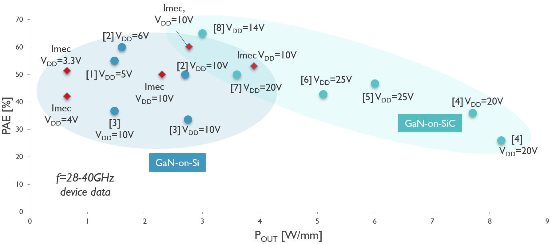
Complementing the technology development with modeling activities will ultimately help achieve even better performance and reliability. For example, at IEDM 2022, imec introduced a simulation framework to predict thermal transport in RF devices better. In a case study with GaN-on-Si HEMTs, the simulations revealed peak temperature rises up to three times larger than previously predicted. Modeling work such as this provides further guidance in optimizing RF devices and their layouts early in the development phase.
Exploring InP-on-Si for 6G sub-THz frequencies: three fabrication approaches
On the longer term, InP HBTs are explored for 6G applications. As previously demonstrated, InP HBTs offer the best output power/efficiency trade-off at 140GHz operating frequency of all technology implementations. Researchers also know how to design InP HBTs for optimal RF performance. But the fabrication usually starts from small (InP) substrate wafers (< 150mm), using lab-like processes that are not CMOS-compatible.
But what happens to the performance when we integrate InP on Si? Depositing InP on Si is known to introduce many defects, mainly threading dislocations and planar defects. These defects induce leakage currents, which can dramatically deteriorate device performance or cause reliability issues.
Three approaches are being considered for upscaling. Two of them rely on the direct growth of InP on Si, and another on wafer reconstruction. All three approaches are envisioned to offer more cost-effective solutions than current technologies that use small InP substrates. But they all have pros and cons regarding performance, cost, and heterogeneous integration potential. Imec has taken on the role of assessing benefits and challenges for the various use cases – infrastructure as well as mobile devices.
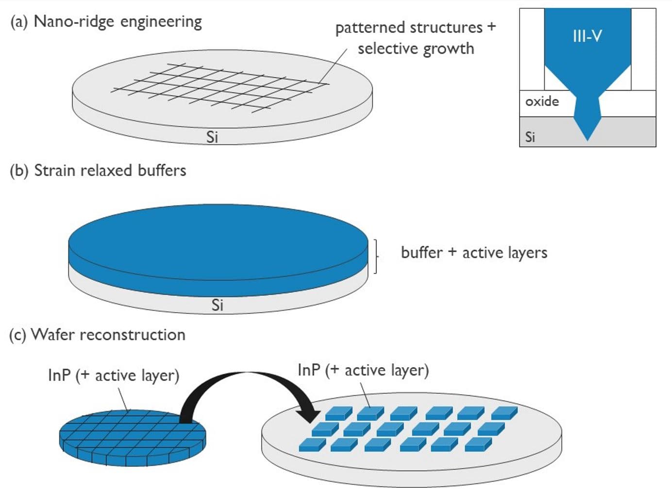
A first approach (Figure 4b) to making InP-on-Si HBTs uses strain-relaxed buffer layers deposited directly on top of Si to compensate for the eight percent lattice mismatch between Si and InP. Next, InP is grown directly on top of this buffer layer. The ability to use larger wafer sizes, especially in cases where some of the Si could be reused, provides a significant cost advantage. However, optimizations are needed to reduce the number of defects further.
Departing from this ‘blanket’ growth approach, imec proposes nano-ridge engineering (NRE) as an alternative technology to cope with defects more efficiently (Figure 4a). NRE relies on selectively growing the III/V material in pre-patterned trenches in Si. These high-aspect-ratio trenches are very effective in trapping the defects in the narrow bottom part and allowing the growth of high-quality, low-defectivity material out of the trench. Overgrowing the nano-ridge widens it towards the top, forming a solid base for a device stack. The first insights obtained from a GaAs/InGaP case study will guide the optimization of the target InGaAs/InP NRE HBT devices.

Beyond direct growth, InP can also be placed on Si using a wafer reconstruction technology (Figure 4c). In this case, high-quality InP substrates – with or without the active layers – are diced into tiles during wafer constitution. The tiles are subsequently attached to a Si wafer using a die-to-wafer bonding technique. The key challenges lie in the efficient transfer of the materials and the removal of the InP substrate, for which several techniques are being considered.
Towards heterogeneous integration
Ultimately, the III/V-on-Si power amplifiers must be combined with CMOS-based components that take care of, e.g., calibration and control. Imec is looking into variousheterogeneous integration options, weighing their pros and cons for various use cases.
Advanced laminate substrate technology is the most common way to integrate different RF components in a system-in-package, and optimizations to make it amendable to higher frequencies are ongoing.
Besides, imec explores more advanced heterogeneous integration options, including 2.5D interposer and 3D integration technologies.
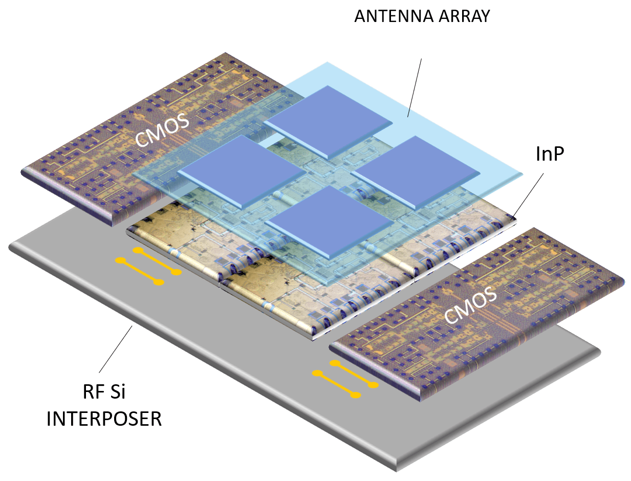
Especially for frequencies above 100GHz, it is important to note that the antenna module starts to define the area available for the transceiver. Indeed, when going to higher frequencies, the wavelength decreases, and the area of the antenna array scales accordingly. Above 100GHz, the antenna size becomes smaller than the front-end module size, which hardly scales in size with increasing frequency. An interesting option for large antenna array configurations is to move the RF front-end module under the antenna array. And this is where 3D integration technologies (either die-to-wafer or wafer-to-wafer) come into play, enabling short and well-defined connections between the front-end module and the antenna modules. However, thermal management remains a great concern for 3D integration, and being able to provide effective heatsinks will be crucial. Today, at imec, we are performing a comprehensive system-technology-co-optimization (STCO) analysis to evaluate different technologies for 3D integration and to guide the technology choices from a system-level perspective.
For handheld devices, where a reduced number of antennas can relax the constraints, 2.5D interposer technology is considered an interesting approach. This heterogeneous integration option uses a layer stack with lithography-defined connections and even through-Si vias to communicate between III/V- and CMOS-based components. In this case, the III/V devices sit next to the CMOS chip, enabling better thermal management because both chips can be in direct contact with a heat sink. Such architecture, however, only allows for 1D beam steering. We are currently evaluating hardware implementations of 2.5D interposer technology, looking into the most optimal combinations of substrates, dielectrics, and redistribution layers to minimize losses. For example, we have shown a first version of an RF-tailored Si interposer technology using a standard Si substrate, copper semi-additive interconnect, and thick spin-on low-k dielectrics that exhibit very low interconnect loss, even above 100GHz.
In summary, recent upscaling and integration efforts show that GaN-on-Si and InP-on-Si can become viable technologies for next-generation high-capacity wireless communication applications.
This article was originally published in Compound Semiconductor (pgs 46-51).
Want to know more?
Imec’s work on GaN and InP is described in the following 2022 IEDM papers. Interested in receiving the papers? Fill in our contact form.
‘Thermal modeling of GaN & InP RF devices with intrinsic account for nanoscale transport effects,’ B. Vermeersch et al., 2022 International Electron Devices Meeting (IEDM).
‘III-V/III-N technologies for next-generation high-capacity wireless communication,’ N. Collaert et el., 2022 International Electron Devices Meeting.
Authors

Nadine Collaert
Nadine Collaert is program director at imec and responsible for the High-speed analog/RF program. She received an M.S. and Ph.D. degree in electrical engineering from the ESAT Department, KU Leuven, Belgium, in 1995 and 2000, respectively. Since then, she has been involved in the theory, design and technology of FinFET devices, emerging memory devices, transducers for biomedical applications and the heterogeneous integration of new materials with Si.
Discover more
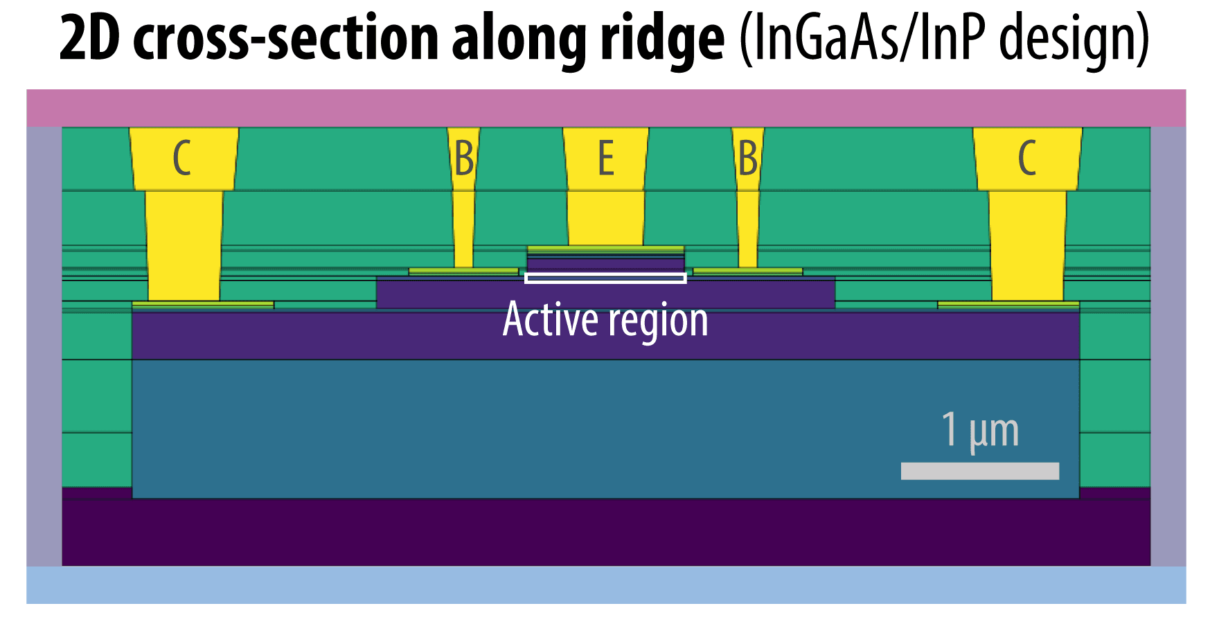
Imec introduces simulation framework to better predict thermal transport in RF devices for 5G and 6G.
Read more