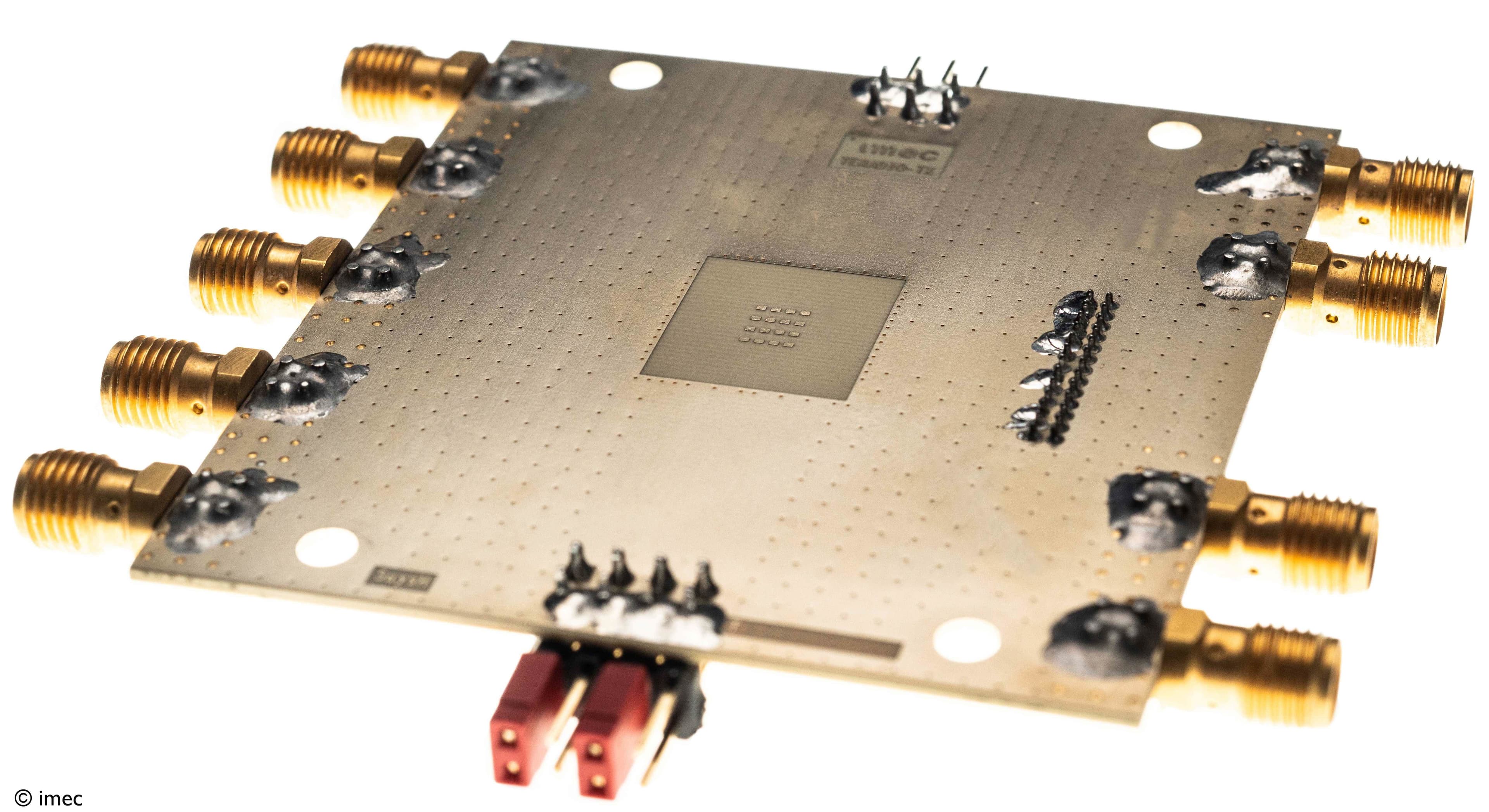
Imec unlocks system-level III-V chiplet integration on Si-CMOS by advancing its 300mm RF silicon interposer platform with high-density MIMCAPs, passive modeling, and laser-assisted bonding

LEUVEN (Belgium), JUNE 11, 2026 — Imec, a world-leading research and innovation hub in advanced semiconductor technologies, is evolving its 300mm RF silicon interposer into a system-level platform for the heterogeneous integration of III-V chiplets on Si-CMOS. By uniquely combining high-density embedded capacitors, a scalable modeling framework for passive components, and laser-assisted bonding for III-V chiplet assembly, the platform lays the foundation for next-generation wireless (mmWave and sub-THz) systems, as well as RF-grade signal handling for ultrafast data center applications.
As wireless systems move into mmWave and sub-THz frequencies, and electronic and photonic interfaces in data centers are increasingly reaching their limits, it is becoming more difficult to deliver high-performance signal handling without driving up system integration complexity, cost, power consumption, and footprint.
A promising solution is to combine the superior gain, power, and efficiency of III-V materials – such as InP, GaAs, and GaN – with the scalability and cost efficiency of Si-CMOS technology. Chiplet-based heterogeneous integration on a high-performance RF silicon interposer makes this possible: it keeps performance-critical functions in compact III-V chiplets, while the interposer provides low-loss interconnects and hosts the remaining passive components.
Imec has been steadily advancing such a platform. In 2024, it demonstrated seamless InP chiplet integration on a 300mm RF silicon interposer with negligible insertion loss at 140GHz. In 2025, it extended the platform’s record-low insertion loss up to 325GHz. Now, imec expands this platform with three new, complementary enablers: high-density embedded capacitors, a scalable modeling framework for passive components, and laser-assisted bonding for III-V chiplet assembly.
A 10-to-100-fold increase in MIMCAP capacitance density for high compactness and cost efficiency
“A key lever to reduce III-V chiplet size and cost is the offloading of passive components – such as decoupling capacitors – onto the RF silicon interposer,” said Xiao Sun, principal member of technical staff at imec. “In a paper presented at this year’s IMS/RFIC conference, we demonstrate how combining this offloading approach with a new MIMCAP architecture enables a 10-to-100-fold increase in capacitance density compared to typical on-chip capacitors in III-V technologies. This supports more compact and cost-efficient system designs and improves power delivery for mmWave and sub-THz wireless systems as well as high-speed data center applications.”
Imec’s new MIM capacitor (MIMCAP) architecture combines a high-k aluminum-hafnium-oxide dielectric with three-dimensional (3D) oxide-stud structures in the back-end-of-line (BEOL).
A modeling framework for predictable design of passive components up to sub-THz frequencies
Complementing this effort, imec recently presented a modeling framework for RF interposer passives, validated up to the sub-THz regime (~300GHz). Imec’s model enables designers to accurately predict circuit performance as geometries change, without needing to re-simulate or measure every variation, significantly reducing development time.
To date, imec’s framework has focused on transmission line performance – but lays the foundation for a comprehensive design library that is being extended to other passive components, including inductors and MIMCAPs.
Laser-assisted bonding enables assembly of passive-rich III-V chiplet systems
Finally, imec demonstrated the use of laser-assisted bonding to integrate III-V chiplets onto its RF silicon interposer, enabling assembly of chiplets on a complex, passives-rich stack without compromising thermal budgets, or damaging temperature-sensitive interposer layers.
Imec’s approach achieves alignment accuracy below 600nm, and rotational misalignment below 0.05° across 43 devices. RF measurements confirm preserved performance after assembly, with reflection below −15 dB in the 110-170GHz range, demonstrating a viable path toward fully assembled high-frequency chiplet-based systems.
Xiao Sun: “With this work, we demonstrate a uniquely integrated platform that brings together performance, scalability, and manufacturability. Our next priority is to further advance the platform’s technology readiness, and to enable support for low-volume manufacturing – helping our partners more easily develop and scale next-generation RF systems.”
Want to know more? Further technical details can be found in imec’s recent conference papers presented at IMS and ECTC 2026.
About imec
Imec is a world-leading research and innovation hub in advanced semiconductor technologies. Leveraging its state-of-the-art R&D infrastructure and the expertise of over 6,500 employees, imec drives innovation in semiconductor and system scaling, artificial intelligence, silicon photonics, connectivity, and sensing.
Imec’s advanced research powers breakthroughs across a wide range of industries, including computing, health, automotive, industry, consumer electronics, aerospace and security. Through IC-Link, imec delivers customized solutions, from concept to full-scale manufacturing, to meet the most advanced design and production needs. Through imec.ventures, imec creates, co‑creates new ventures, and supports existing semiconductor deep‑tech companies to scale-up.
Imec collaborates with global leaders across the semiconductor value chain, as well as with technology companies, start-ups, academia, and research institutions in Flanders and worldwide. Headquartered in Leuven, Belgium, imec has research facilities in Belgium, across Europe, the USA and the GCC region, and representation on three continents. In 2025, imec reported revenues of €1.2 billion.
For more information, visit www.imec-int.com
The imec group holds a global trademark portfolio, including word marks and combined figurative registered and unregistered trademarks, across national, regional, and international territories. Its lawful use requires prior written consent of IMEC in compliance with the IMEC branding guidelines, which may be updated periodically. The latest version is available upon written request.
Discover more

Imec achieves record-breaking RF GaN-on-Si transistor performance for high-efficiency 6G power amplifiers
Read more
Imec presents 150 GSa/s Digital-to-Analog Converter (DAC) achieving 300 Gb/s data transmission
Read more
Imec and Ghent University present a fully-integrated, single-chip microwave photonics system for compact and versatile signal processing
Read more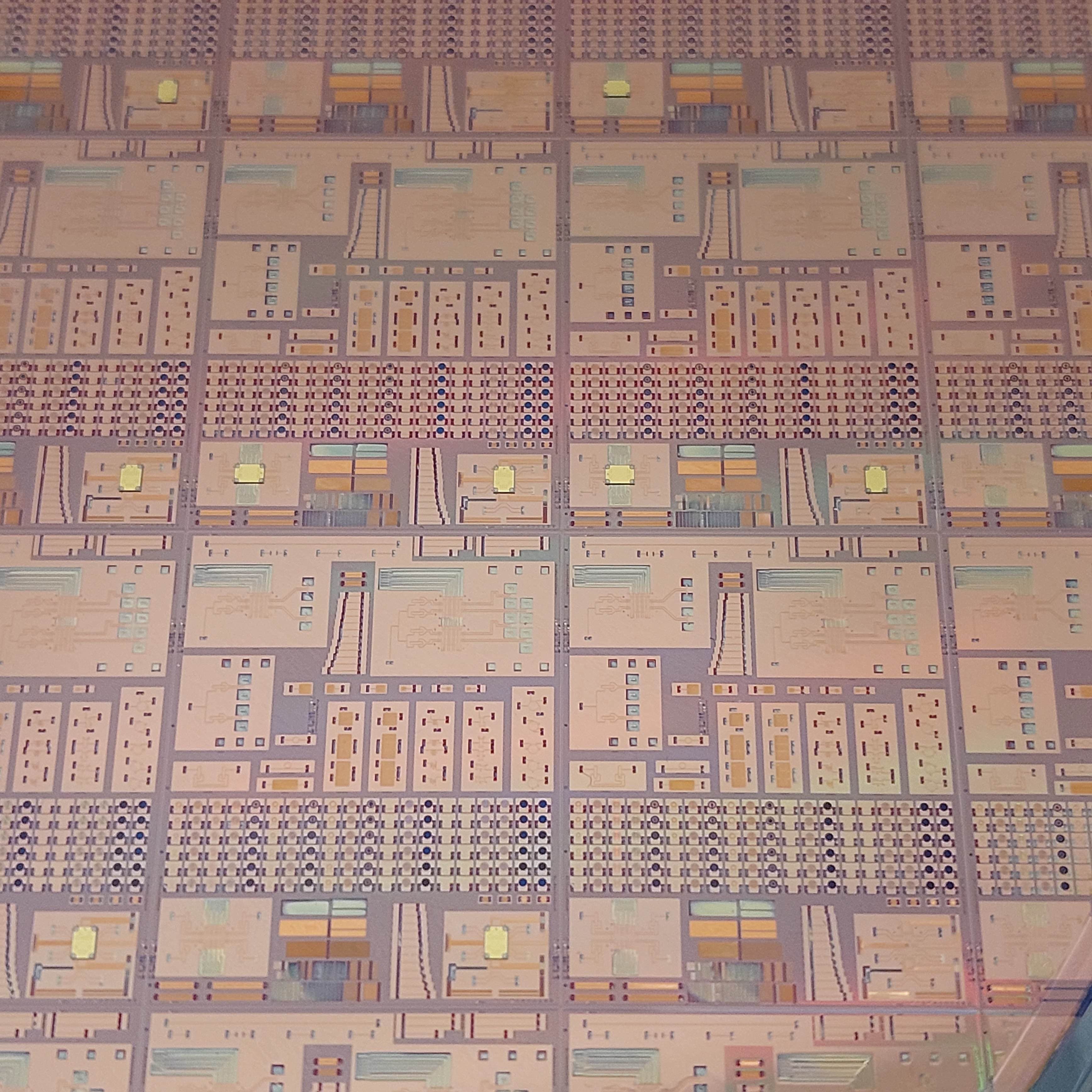
300mm RF silicon interposer platform for chiplet-based heterogeneous integration demonstrates record-low insertion loss at frequencies up to 325GHz
Read more
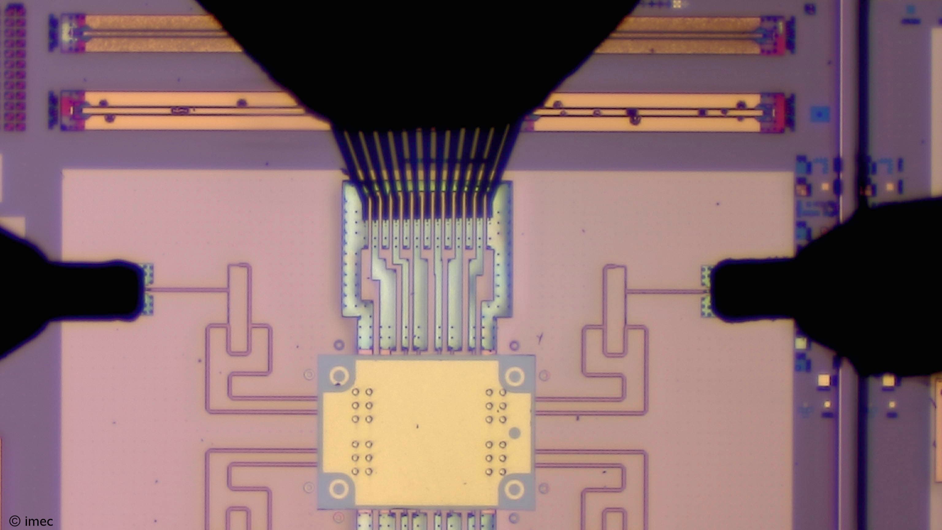
Imec achieves seamless InP Chiplet integration on 300mm RF Silicon Interposer with excellent performance at 140GHz
Read more
Imec introduces best-in-class ADCs for base stations and smartphones, propelling beyond-5G communications
Read more