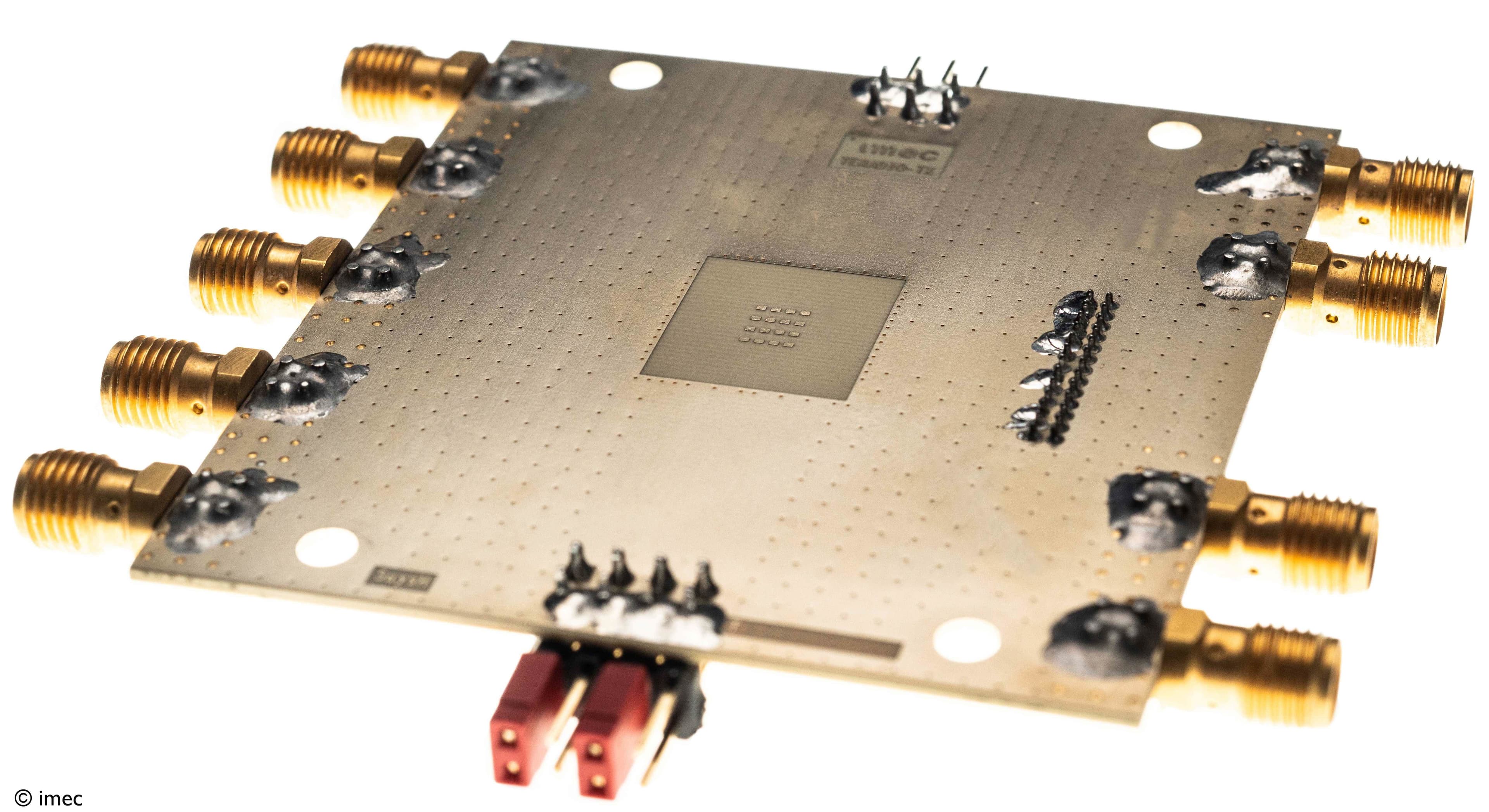
Imec presents 150 GSa/s Digital-to-Analog Converter (DAC) achieving 300 Gb/s data transmission
High-speed DAC paves the way for faster and more energy-efficient optical and electrical links in data centers
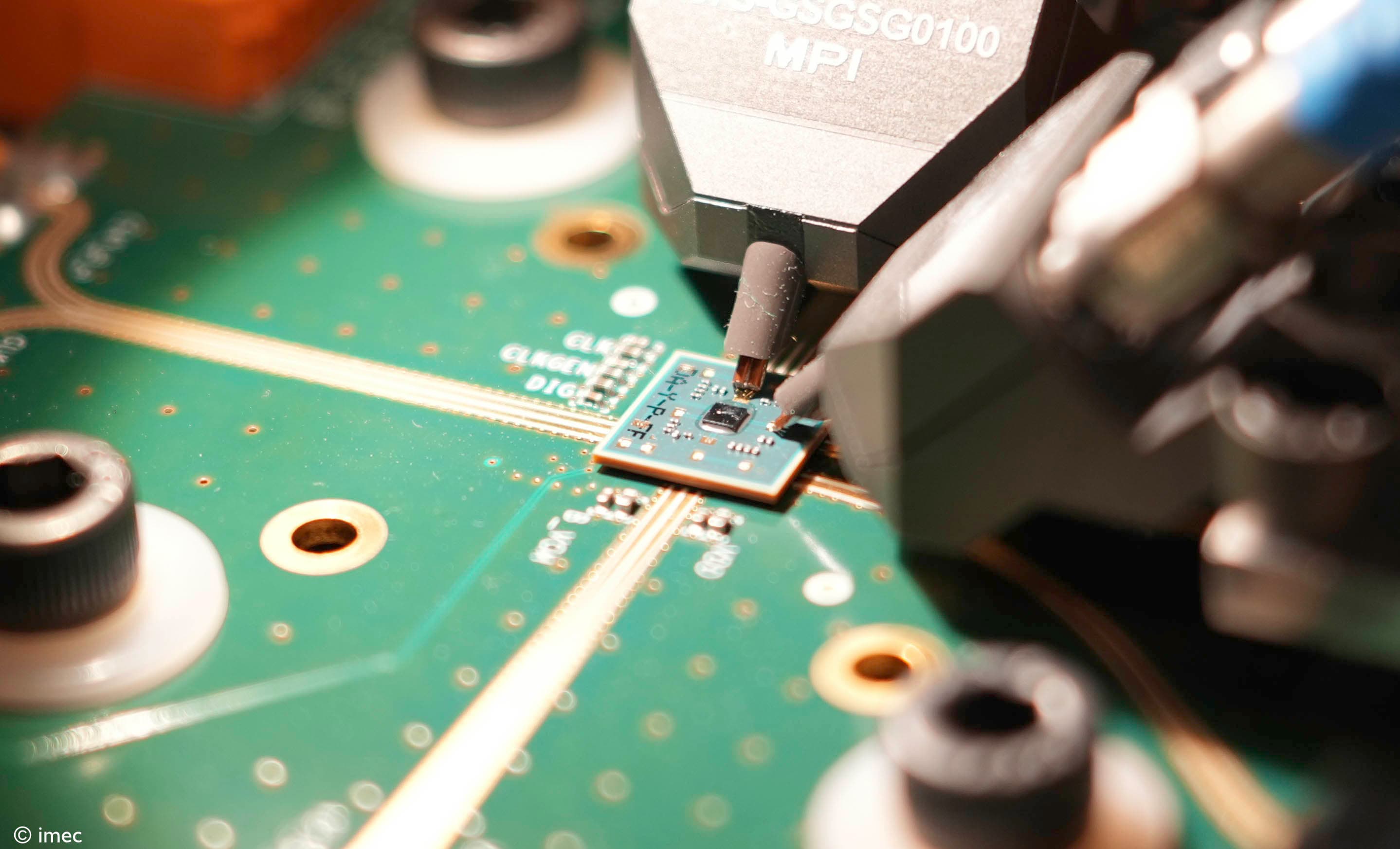
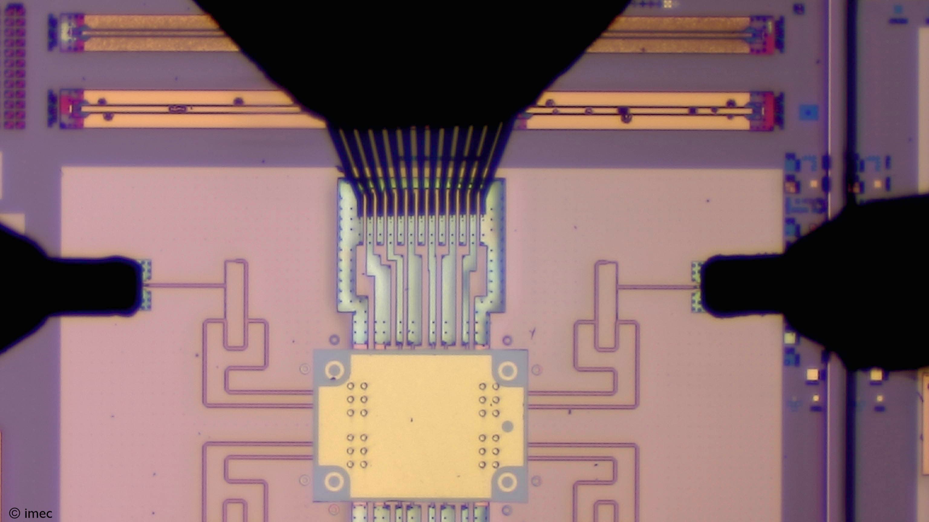
LEUVEN (Belgium), JUNE 11, 2025— This week at the 2025 Symposium on VLSI Technology and Circuits, imec, a world-leading research and innovation hub in nanoelectronics and digital technologies, and IDLab, an imec research group at Ghent University and the University of Antwerp, Belgium, announced a significant breakthrough in high-speed digital-to-analog conversion. The new 7-bit 150 GSa/s Digital-to-Analog Converter (DAC), fabricated in a 5nm FinFET CMOS process, achieves data rates of up to 300 Gb/s using PAM-4 modulation. Designed to address the growing demand for faster data center links, the DAC combines speed and power efficiency, setting a new standard for wireline data conversion.
The demand for higher data transfer rates in data centers continues to surge as data-intensive applications like machine learning and AI become more prevalent. To handle the vast amounts of data flowing through these centers, wireline communication systems rely on analog-to-digital converters (ADCs) and digital-to-analog converters (DACs) to convert analog signals to digital data and back, allowing the use of sophisticated signal processing supporting transmission over physical links. However, as data volumes continue to rise, ADCs and DACs must convert data at increasingly higher speeds to ensure efficiency. Ultra-fast ADCs and DACs are therefore essential to ensure data flow in next-generation wireline systems. Conventional architectures often fall short, resulting in signal degradation and power inefficiencies. At the same time, power efficiency is becoming increasingly important, as the amount of interconnect deployed inside large-scale data center infrastructures grows at an even faster pace than the amount of compute.
Imec’s latest DAC addresses these challenges by achieving a high-speed 150 GSa/s sample rate, capable of generating data rates up to 300 Gb/s using PAM-4. With increasing data rates, PAM-4 has emerged as the preferred modulation scheme in data centers, enabling faster data transfer without requiring more bandwidth. “This 7-bit DAC is designed for next-generation data center links, targeting data rates above 200 Gb/s and ultimately reaching 400 Gb/s per lane. In order to efficiently manage these speeds, the necessary signal processing is implemented in advanced CMOS nodes such as 5nm FinFET. Consequently, the DAC must also be realized within the same technology node. Integrating such complex architectures in scaled CMOS nodes draws on imec’s unique expertise in advanced integrated circuit design,” says Peter Ossieur, program manager for high-speed transceivers at imec.
To optimize power efficiency, imec has innovated the DAC architecture by drastically reducing the number of unit cells from 127 to 34. This has minimized switching activity, effectively lowering power consumption (to 621 mW at 0.9V and 0.96V supplies) without compromising speed. This reduction also decreases parasitic effects, enabling more accurate signal conversion at higher data rates.
Ossieur added: “Looking ahead, the team aims to address the growing demand for even faster data links by targeting the next generation of ADCs and DACs based on 3nm CMOS technology. The focus is on doubling the sampling rate to 300GSa/s and pushing bandwidth beyond 100GHz. To achieve such speed imec will draw on its expertise in analog design, and now also addresses the design of ultra-low-jitter clock generation circuitry targeting femtosecond-level accuracies.”
About imec
Imec is a world-leading research and innovation center in nanoelectronics and digital technologies. Imec leverages its state-of-the-art R&D infrastructure and its team of more than 6.000 employees and top researchers, for R&D in advanced semiconductor and system scaling, silicon photonics, artificial intelligence, beyond 5G communications and sensing technologies, and in application domains such as health and life sciences, mobility, industry 4.0, agrofood, smart cities, sustainable energy, education, … Imec unites world-industry leaders across the semiconductor value chain, Flanders-based and international tech, pharma, medical and ICT companies, start-ups, and academia and knowledge centers. Imec is headquartered in Leuven (Belgium), and has research sites across Belgium, in the Netherlands, the UK and the USA, and representation in 3 continents. In 2024, imec's revenue (P&L) totaled 1,034 billion euro.
Further information on imec can be found at www.imec-int.com.
The imec group holds a global trademark portfolio, including word marks and combined figurative registered and unregistered trademarks, across national, regional, and international territories. Its lawful use requires prior written consent of IMEC in compliance with the IMEC branding guidelines, which may be updated periodically. The latest version is available upon written request.
Discover more
Imec unlocks system-level III-V chiplet integration on Si-CMOS by advancing its 300mm RF silicon interposer platform with high-density MIMCAPs, passive modeling, and laser-assisted bonding
Read more
Imec achieves record-breaking RF GaN-on-Si transistor performance for high-efficiency 6G power amplifiers
Read more
Imec and Ghent University present a fully-integrated, single-chip microwave photonics system for compact and versatile signal processing
Read more
300mm RF silicon interposer platform for chiplet-based heterogeneous integration demonstrates record-low insertion loss at frequencies up to 325GHz
Read more
Imec achieves seamless InP Chiplet integration on 300mm RF Silicon Interposer with excellent performance at 140GHz
Read more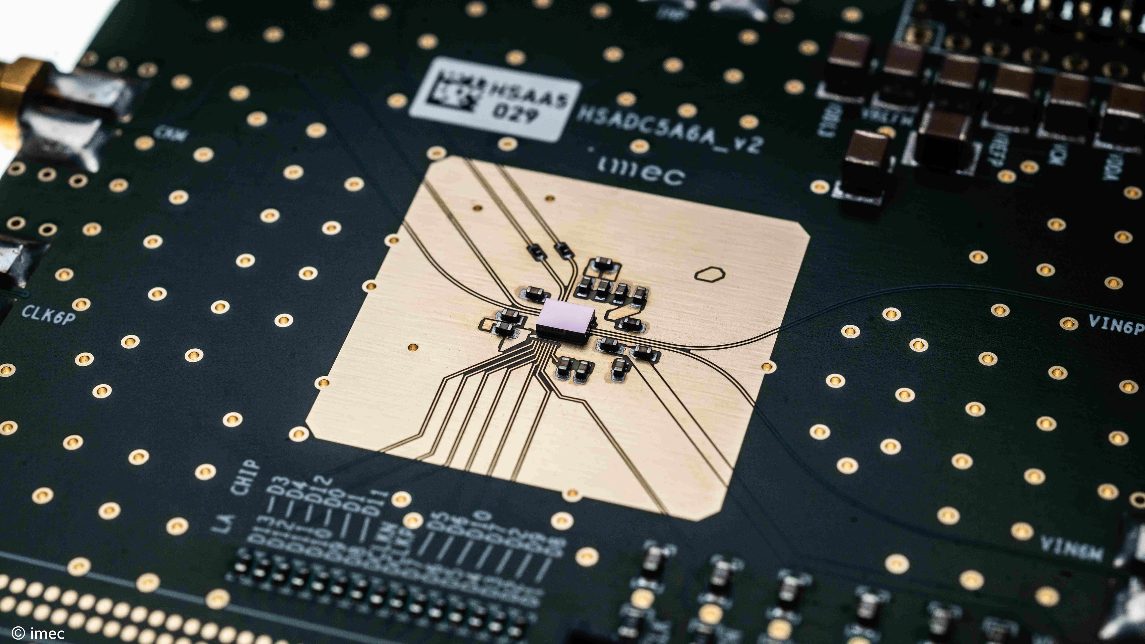
Imec introduces best-in-class ADCs for base stations and smartphones, propelling beyond-5G communications
Read more