Imec achieves seamless InP Chiplet integration on 300mm RF Silicon Interposer with excellent performance at 140GHz
Using RF silicon interposer technology to combine high-performance III-V chiplets with silicon-based wafer-scale packaging paves the way for cost-effective mmWave communication and sensing
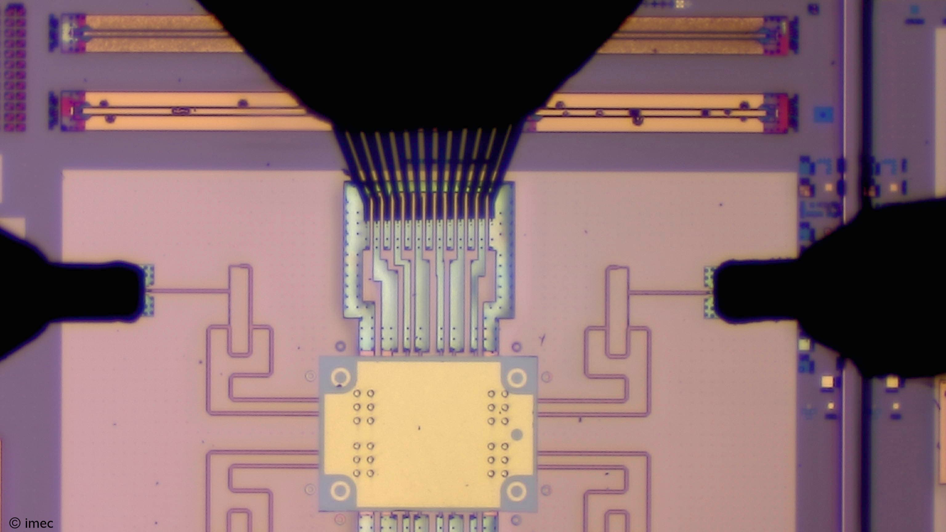
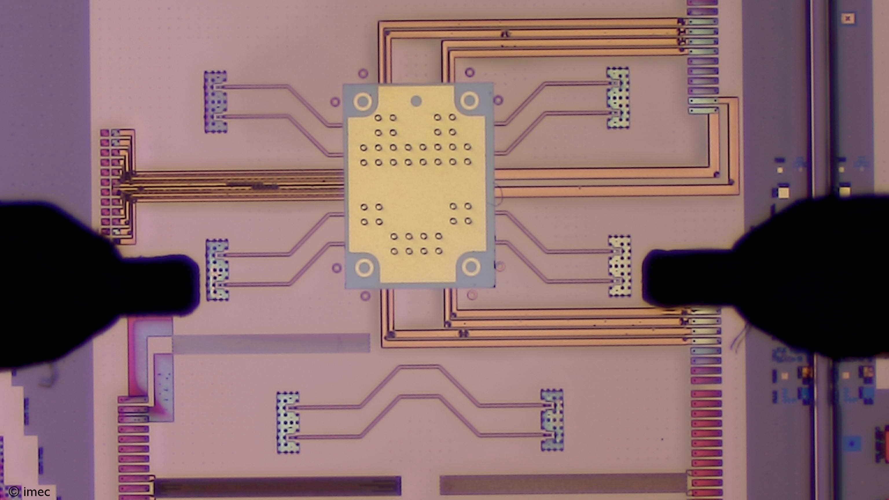
LEUVEN (Belgium), DECEMBER 9, 2024 — At this week’s IEEE International Electron Devices Meeting (IEDM), imec – a world-leading research and innovation hub in nanoelectronics and digital technologies – presents breakthrough results in the hetero-integration of InP chiplets on a 300mm RF silicon interposer. The chiplets’ integration comes with a negligible 0.1dB insertion loss at 140GHz. In addition, researchers observe zero performance degradation upon assembly of a two-stage InP power amplifier (PA). As the first to achieve this, imec’s findings mark a significant milestone in developing compact, energy-efficient modules for above 100GHz communication and radar sensing.
To meet the demand for faster data transfer, increased bandwidth, and advanced imaging, next-generation communication and (radar) sensing systems must utilize higher frequency bands. This shift requires compact, cost-optimized, and energy-efficient components that operate at higher speeds and deliver more output power than current technologies.
Imec sees heterogeneous III-V/Si-CMOS technology as a promising path forward, with indium phosphide (InP) showing particular potential thanks to its high gain and power efficiency at mmWave and sub-THz frequencies. However, current InP technology has several drawbacks that limit its application to niche markets, such as the use of small-sized wafers and processing via E-beam lithography, while a large portion of the design area is occupied by passives and gold-based backends.
“By using InP only where its unmatched performance is essential, imec is paving the way toward scalable, cost-effective mmWave and sub-THz solutions. This is where a chiplet approach becomes essential,” explains Siddhartha Sinha, a principal member of technical staff at imec.
RF silicon interposer and InP chiplet integration shows 0.1dB insertion loss at 140GHz, with no performance degradation upon assembly of an InP PA
Building on its leadership in silicon interposer technology, imec has adapted its expertise in 2.5 technology to enable next-gen RF applications, delivering ultra-low loss and compact integration for mmWave and sub-THz signals.
Siddhartha Sinha: “Silicon interposer technology has been pivotal for digital and HPC use cases. Imec has extensive expertise in developing the underlying enablers, such as scaled micro-bumps, high-aspect-ratio TSVs, and multi-layer Cu damascene routing to meet these applications’ high-density routing needs. And leveraging this knowledge, we have now adapted silicon interposer technology to suit RF applications by adding small, high-performance InP chiplets using CMOS-like processes.”
Imec’s RF interposer adds low-loss RF layers on top of a digital interposer to route mmWave signals. Utilizing small-footprint interconnects with a 40µm flip-chip pitch, the passive interconnects between the InP chiplets and the RF interposer show a 0.1dB insertion loss at 140GHz—which is negligible. In addition, a two-stage InP power amplifier (PA) demonstrates excellent performance with no degradation observed after assembly, validating the effectiveness of the InP chiplet approach.
The path forward: making InP compatible with CMOS processing modules and toolsets
Building on the results presented at IEDM, imec researchers continue to explore further interposer advancements as part of a broader program to make InP compatible with CMOS processing modules and toolsets.
“In addition to developing a demonstrator for mmWave phased arrays and radar applications, we aim to further shrink the size of the InP chiplets while preserving their superior RF performance. We also plan to add new Si RF interposer features to the platform, including passives like inductors and MIMCAPs, as well as TSV integration and wafer thinning,” said Sinha.
“At the same time, we’re making the platform available to partners for prototyping, allowing them to experiment with imec’s RF interposer R&D platform,” he concludes.
These research results will be discussed in-depth on Monday, December 9 from 1:35 PM to 2:00 PM (PST) during a technical session at this year’s IEDM.
About imec
Imec is a world-leading research and innovation center in nanoelectronics and digital technologies. Imec leverages its state-of-the-art R&D infrastructure and its team of more than 5,500 employees and top researchers, for R&D in advanced semiconductor and system scaling, silicon photonics, artificial intelligence, beyond 5G communications and sensing technologies, and in application domains such as health and life sciences, mobility, industry 4.0, agrofood, smart cities, sustainable energy, education, … Imec unites world-industry leaders across the semiconductor value chain, Flanders-based and international tech, pharma, medical and ICT companies, start-ups, and academia and knowledge centers. Imec is headquartered in Leuven (Belgium), and has research sites across Belgium, in the Netherlands, the UK and the USA, and representation in 3 continents. In 2023, imec's revenue (P&L) totaled 941 million euro.
Further information on imec can be found at www.imec-int.com.
Imec is a registered trademark for the activities of imec International and its affiliated entities.
Discover more
300mm RF silicon interposer platform for chiplet-based heterogeneous integration demonstrates record-low insertion loss at frequencies up to 325GHz
Read more
Imec unveils CMOS-based 56Gb/s zero-IF D-band beamforming transmitter, featuring superior output power and energy efficiency
Read more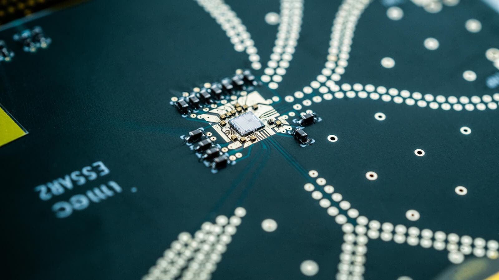
Imec Unveils Breakthrough ADC Architecture for Very High-Speed Wireline Applications, Excelling in Area & Power Efficiency
Read more
Imec unlocks system-level III-V chiplet integration on Si-CMOS by advancing its 300mm RF silicon interposer platform with high-density MIMCAPs, passive modeling, and laser-assisted bonding
Read more
Imec achieves record-breaking RF GaN-on-Si transistor performance for high-efficiency 6G power amplifiers
Read more
Imec presents 150 GSa/s Digital-to-Analog Converter (DAC) achieving 300 Gb/s data transmission
Read more