Imec Unveils Breakthrough ADC Architecture for Very High-Speed Wireline Applications, Excelling in Area & Power Efficiency
Imec’s massively time-interleaved slope-ADC prototype chip demonstrates superior scalability to meet data centers’ exploding bandwidth and data processing demands
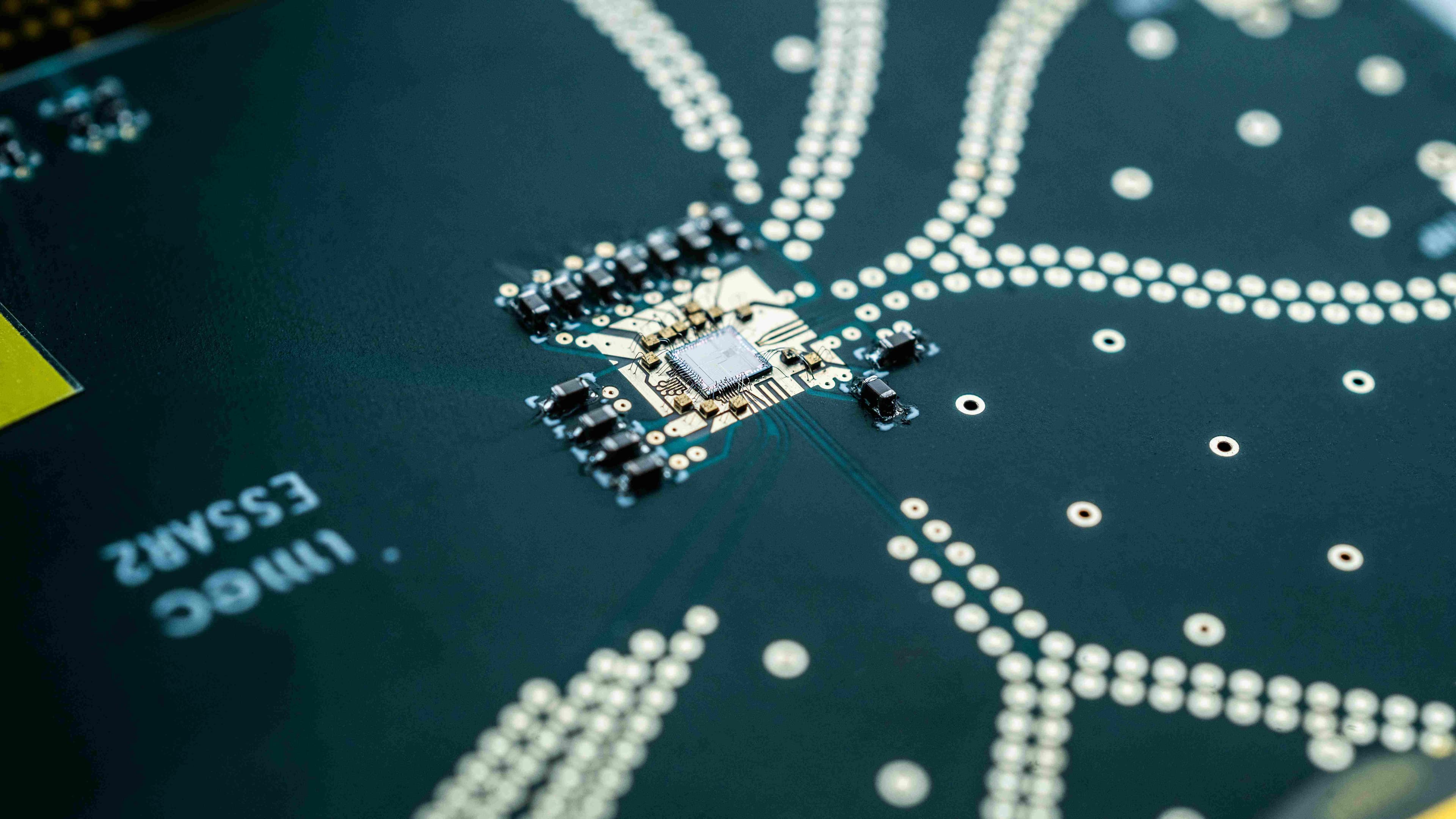
LEUVEN (Belgium), FEBRUARY 21, 2024 — At this week’s IEEE International Solid-State Circuits Conference (IEEE ISSCC2024), imec – a world-leading research and innovation hub in nanoelectronics and digital technologies – introduces a breakthrough architecture that lays the foundation for a whole new generation of analog-to-digital converters (ADCs). Imec’s massively time-interleaved slope-ADC design offers high power efficiency and a very compact footprint, while promising to enable exceptional conversion speeds. As such, it is ideally suited to meet data centers’ exploding data processing and throughput demands, driven by the surge in cloud computing and (generative) AI applications.
Training AI models requires massive computing power, necessitating data centers to invest in increasingly powerful optical networks for fast, reliable communications between servers, storage devices, and networking equipment. But since data centers' optical communication networks need to operate at higher and higher speeds, their components grow in size and power consumption.
A new architecture that overcomes the limitations of time-interleaved SAR ADCs
A critical component of optical transceivers, today’s wireline ADCs are mostly based on time interleaving of (large numbers of) successive approximation register (SAR) ADCs that feature tens of parallel high-speed channels. As such, when scaling to sampling rates far beyond 100GS/s, the SAR ADC approach results in a significant area increase and long interconnection lines, translating into substantial parasitics and energy loss.
To support the insatiable bandwidth and data processing demands of wireline applications and their need for ever faster ADCs, imec proposes a new ADC architecture that overcomes these limitations.
“On the one hand, our massively time-interleaved slope-ADC design exploits the paradigm that slow-speed, but extremely small channels make for a more efficient conversion per area. Secondly, by arranging (lots of) these channels in a two-dimensional array, the length of the interconnection lines is minimized, and the power dissipated through parasitics is reduced. As a result, higher power efficiency and scalability can be achieved, while significantly reducing the ADC’s surface area,” said Joris Van Driessche, program manager at imec.
Proof-of-concept: a 42GS/s 7b 16nm massively time-interleaved slope-ADC prototype chip
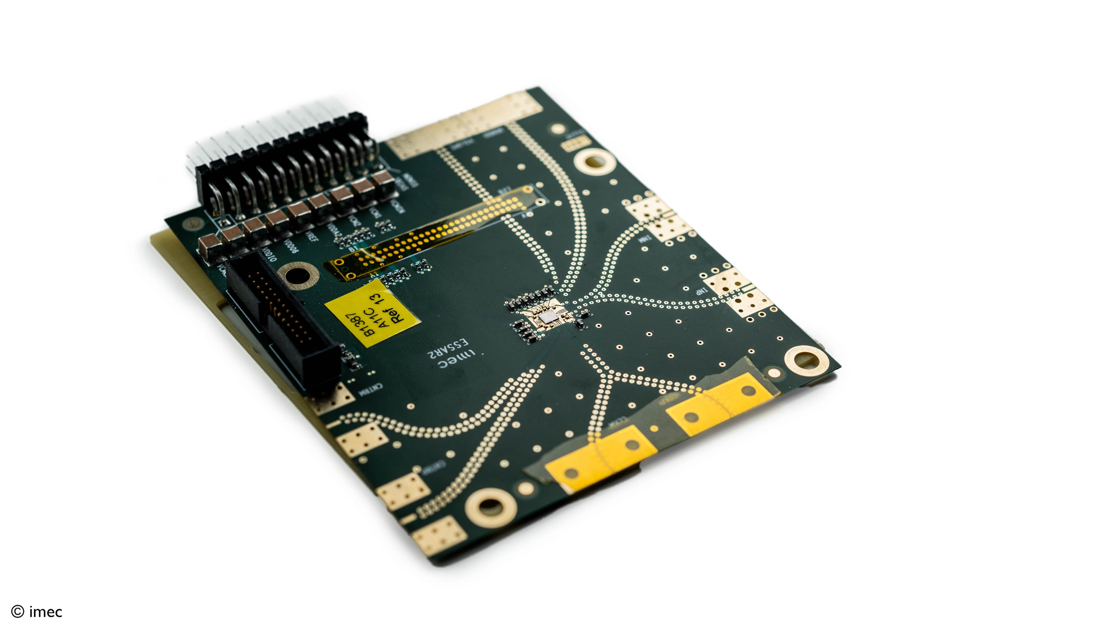
At ISSCC, imec presents a proof-of-concept of its new ADC architecture in the form of a 42GS/s 7b massively time-interleaved slope-ADC prototype chip.
“Even at the relatively modest speed of 42GS/s, the benefits of our approach are clear. Implemented in 16nm FinFET technology, our prototype chip contains an array of 768 slope-ADCs – with a core active area of just 0.07mm². This is at least a factor of two smaller than conventional approaches. It also has a state-of-the-art power consumption of 96mW,” commented Joris Van Driessche. “In other words, this is the first proof that our novel architecture works. And its benefits will only become more significant as we move to higher speeds (150GS/s and beyond).”
In fact, a 5nm ADC using the same architecture is currently being completed – targeting sampling rates well above 150GS/s while achieving extremely low power consumption. In parallel, the team has started exploring a 2nm implementation, targeting speeds in excess of 250GS/s.
“We believe this is an important stepping stone in the development of a whole new generation of small-area, low-power ADCs to support tomorrow’s wireline applications. It overcomes the limitations of SAR ADC implementations, which risk running out of steam when required to operate at extremely high speeds,” concluded Van Driessche.
Imec enthusiastically invites additional partners to join this research effort – such as fabless companies specializing in the development of wireline connectivity building blocks. Moreover, licensing options are available for those companies seeking access to imec’s ADC IP blocks.
Imec has a long track record in developing high-speed integrated circuits for photonics applications. One of its research tracks is aimed at creating optical transceivers (and their various building blocks) that can keep up with the exploding data rates of wireline applications. Late last year, for example, imec researchers at Ghent University developed an optical receiver achieving a gross data rate of 200 Gbps by co-integrating a traveling-wave SiGe BiCMOS transimpedance amplifier with a silicon photonics Ge photodetector to combine the need for speed with a scalable and affordable implementation. The pursuit of a new generation of ADCs and DACs clearly complements this research effort, taking ADC development to a whole new level.
Join us at IEEE ISSCC2024 and discover the future of high-speed ADCs at the imec booth (booth #1).
About imec
Imec is a world-leading research and innovation center in nanoelectronics and digital technologies. Imec leverages its state-of-the-art R&D infrastructure and its team of more than 5,500 employees and top researchers, for R&D in advanced semiconductor and system scaling, silicon photonics, artificial intelligence, beyond 5G communications and sensing technologies, and in application domains such as health and life sciences, mobility, industry 4.0, agrofood, smart cities, sustainable energy, education, … Imec unites world-industry leaders across the semiconductor value chain, Flanders-based and international tech, pharma, medical and ICT companies, start-ups, and academia and knowledge centers. Imec is headquartered in Leuven (Belgium), and has research sites across Belgium, in the Netherlands and the USA, and representation in 3 continents. In 2022, imec's revenue (P&L) totaled 846 million euro.
Further information on imec can be found at www.imec-int.com.
Imec is a registered trademark for the activities of imec International (IMEC International, a legal entity set up under Belgian law as a “stichting van openbaar nut”), imec Belgium (IMEC vzw supported by the Flemish Government), imec the Netherlands (Stichting IMEC Nederland), imec Taiwan (IMEC Taiwan Co.), imec India (IMEC India Private Limited), imec San Francisco (IMEC Inc.) and imec Florida (IMEC USA Nanoelectronics Design Center Inc.).
Discover more
300mm RF silicon interposer platform for chiplet-based heterogeneous integration demonstrates record-low insertion loss at frequencies up to 325GHz
Read more
Imec achieves seamless InP Chiplet integration on 300mm RF Silicon Interposer with excellent performance at 140GHz
Read more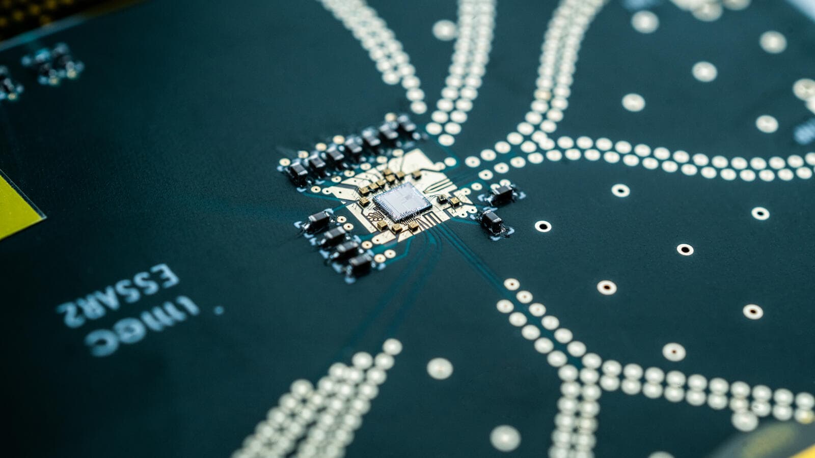
Imec unveils CMOS-based 56Gb/s zero-IF D-band beamforming transmitter, featuring superior output power and energy efficiency
Read more
Imec unlocks system-level III-V chiplet integration on Si-CMOS by advancing its 300mm RF silicon interposer platform with high-density MIMCAPs, passive modeling, and laser-assisted bonding
Read more
Imec achieves record-breaking RF GaN-on-Si transistor performance for high-efficiency 6G power amplifiers
Read more
Imec presents 150 GSa/s Digital-to-Analog Converter (DAC) achieving 300 Gb/s data transmission
Read more