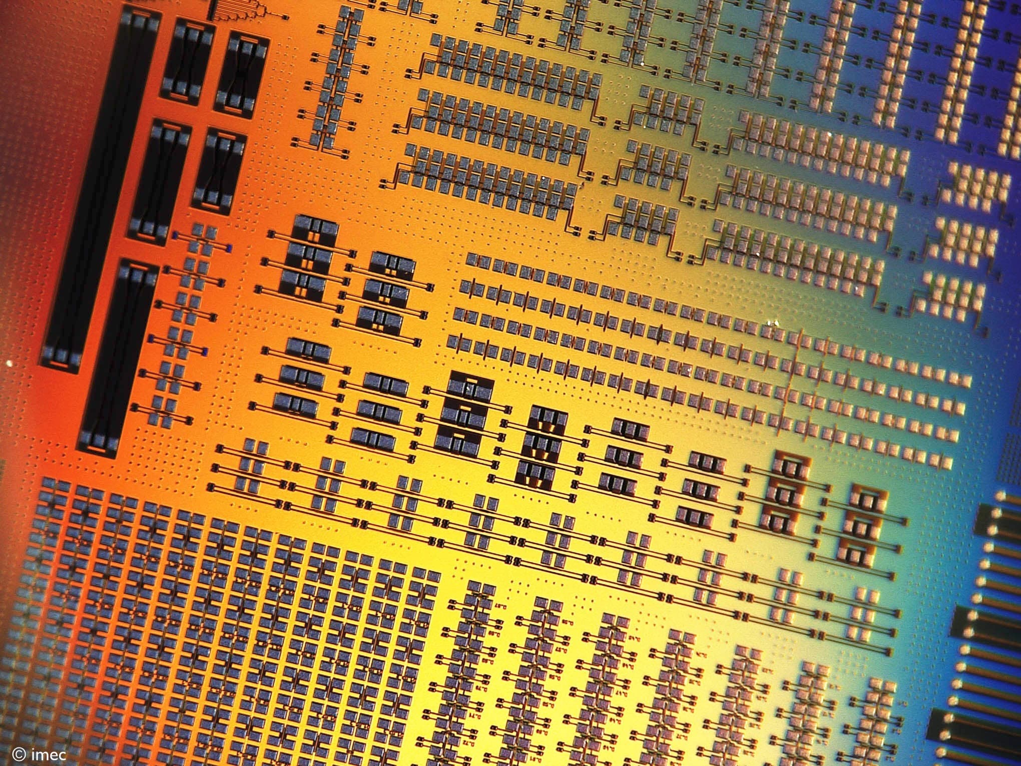
Imec and Ghent University present a fully-integrated, single-chip microwave photonics system for compact and versatile signal processing
A programmable solution for higher-speed wireless communication networks and low-cost microwave sensing

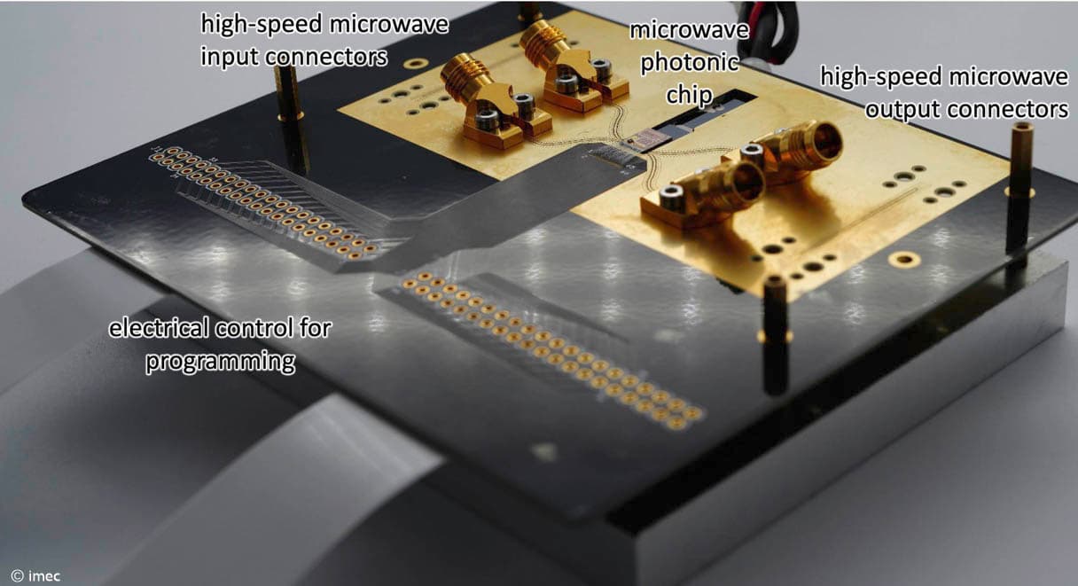
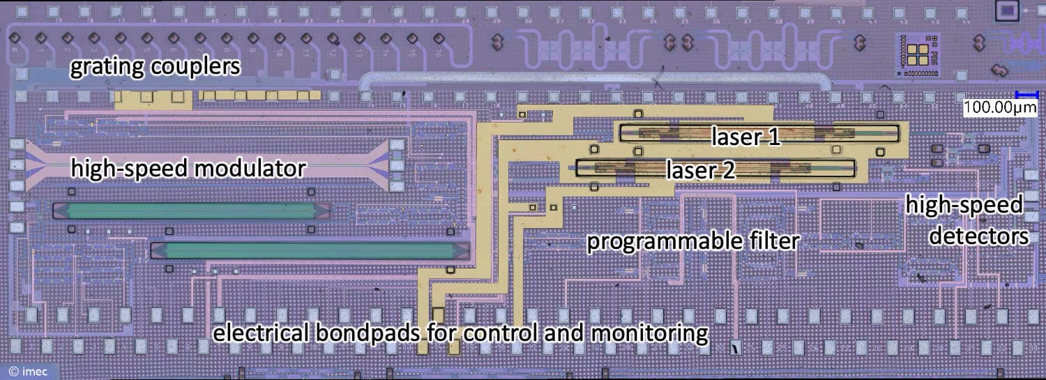
LEUVEN (Belgium), June 5, 2025— This week, the Photonics Research Group and IDlab, two imec research groups at Ghent University, and imec, a world-leading research and innovation hub in nanoelectronics and digital technologies, have published the demonstration of a fully-integrated single-chip microwave photonics system, combining optical and microwave signal processing on a single silicon chip. The chip integrates high-speed modulators, optical filters, photodetectors, as well as transfer-printed lasers, making it a compact, self-contained and programmable solution for high-frequency signal processing. This breakthrough can replace bulky and power-hungry components, enabling faster wireless networks, low-cost microwave sensing, and scalable deployment in applications like 5G/6G, satellite communications, and radar systems. The results have been published in Nature Communications.
Modern communication networks rely on both high-speed fiber-optic links and wireless radio-frequency microwave transmission, but as demand for higher data rates and operation at higher frequencies grows, new systems need much tighter integration between these two modes of communication to overcome the struggle with signal processing complexity, high transmission losses, and power-hungry electronics. Microwave photonics offers a promising solution by using optical technology to process high-frequency signals with lower loss, higher bandwidth, and improved energy efficiency. However, most microwave photonics systems rely on bulky, fiber-based architectures that limit scalability. In contrast, integrating microwave photonics onto a chip could enable more scalable and power-efficient systems, but early experimental demonstrations have either lacked key functionalities or required external components to achieve full performance.
Imec and Ghent University now demonstrate a silicon photonic engine that processes and converts both optical and microwave signals on a single chip. The key innovation in this new system lies in the novel combination of a reconfigurable modulator and a programmable optical filter enabling efficient modulation and filtering of microwave signals while significantly reducing signal loss. This unique combination enhances overall performance allowing the system to handle complex signal processing tasks with greater flexibility and efficiency for a wide range of applications.
The chip is built on imec’s standard iSiPP50G silicon photonics platform, which includes low-loss waveguides and passive components, high-speed modulators and detectors, and thermo-optic phase shifters for tuning the optical response. To provide an integrated light source, the researchers incorporated an indium phosphide (InP) optical amplifier (developed by III-V Lab) on the chip using the microtransfer-printing technology developed at the Photonics Research Group (imec/Ghent University). In combination with on-chip tunable filter circuits, this allows the optical amplifier to function as a widely tunable laser, further enhancing the system’s versatility.
“The ability to integrate all essential microwave photonics components on a single chip marks a major step toward scalable and energy-efficient high-frequency signal processing,” said Wim Bogaerts, professor in the Photonics Research Group at Ghent University and imec. “By eliminating bulky external components, this technology paves the way for more compact, cost-effective solutions in next-generation wireless networks and advanced sensing systems.”
About imec
Imec is a world-leading research and innovation center in nanoelectronics and digital technologies. Imec leverages its state-of-the-art R&D infrastructure and its team of more than 6.000 employees and top researchers, for R&D in advanced semiconductor and system scaling, silicon photonics, artificial intelligence, beyond 5G communications and sensing technologies, and in application domains such as health and life sciences, mobility, industry 4.0, agrofood, smart cities, sustainable energy, education, … Imec unites world-industry leaders across the semiconductor value chain, Flanders-based and international tech, pharma, medical and ICT companies, start-ups, and academia and knowledge centers. Imec is headquartered in Leuven (Belgium), and has research sites across Belgium, in the Netherlands, the UK and the USA, and representation in 3 continents. In 2024, imec's revenue (P&L) totaled 1,034 billion euro.
Further information on imec can be found at www.imec-int.com.
The imec group holds a global trademark portfolio, including word marks and combined figurative registered and unregistered trademarks, across national, regional, and international territories. Its lawful use requires prior written consent of IMEC in compliance with the IMEC branding guidelines, which may be updated periodically. The latest version is available upon written request.
Discover more

Imec unlocks system-level III-V chiplet integration on Si-CMOS by advancing its 300mm RF silicon interposer platform with high-density MIMCAPs, passive modeling, and laser-assisted bonding
Read more
Imec unveils 7‑bit, 175GS/s massively time-interleaved slope-ADC – pairing record-small footprint and low conversion energy with top sampling speed
Read more

Veeco and imec develop 300mm-compatible process to enable integration of barium titanate on silicon photonics
Read more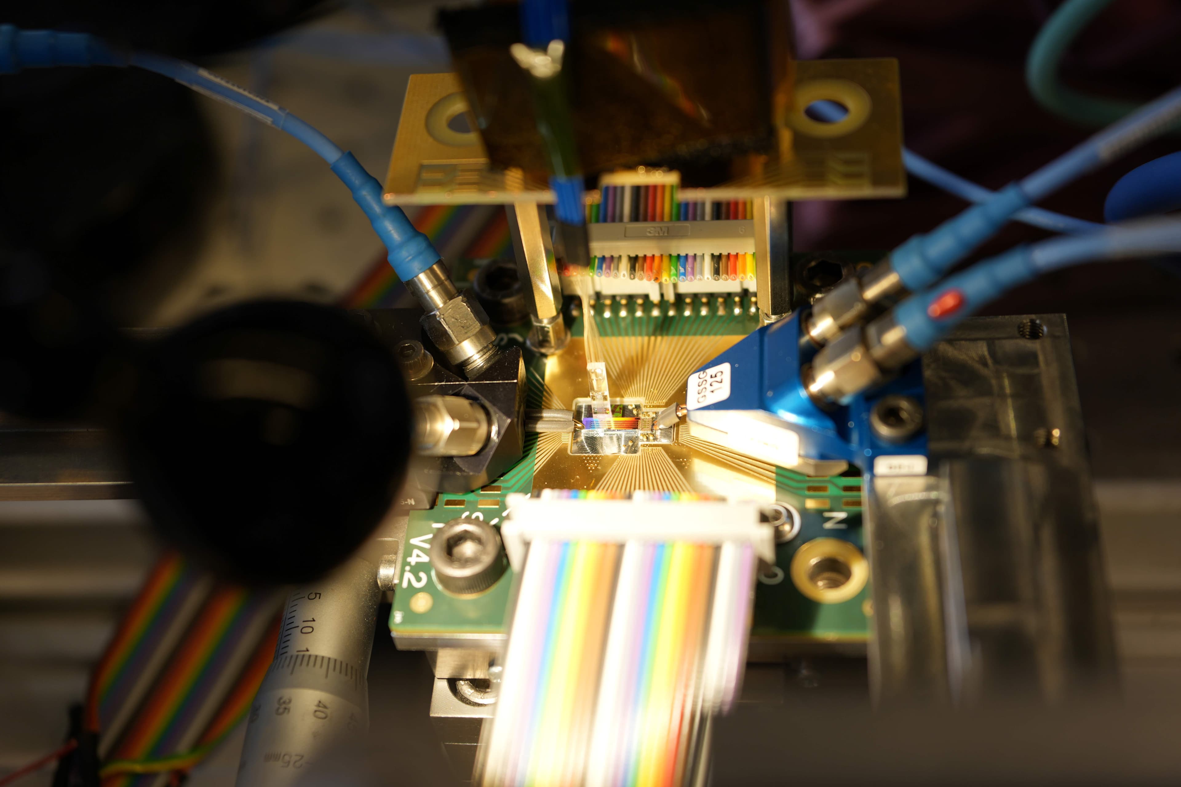
A double world-first: integrating lithium niobate and lithium tantalate modulators on silicon photonics through micro-transfer printing
Read more