Veeco and imec develop 300mm-compatible process to enable integration of barium titanate on silicon photonics
First-of-its-kind solution for barium titanate epitaxy on silicon to accelerate datacom and quantum computing applications.

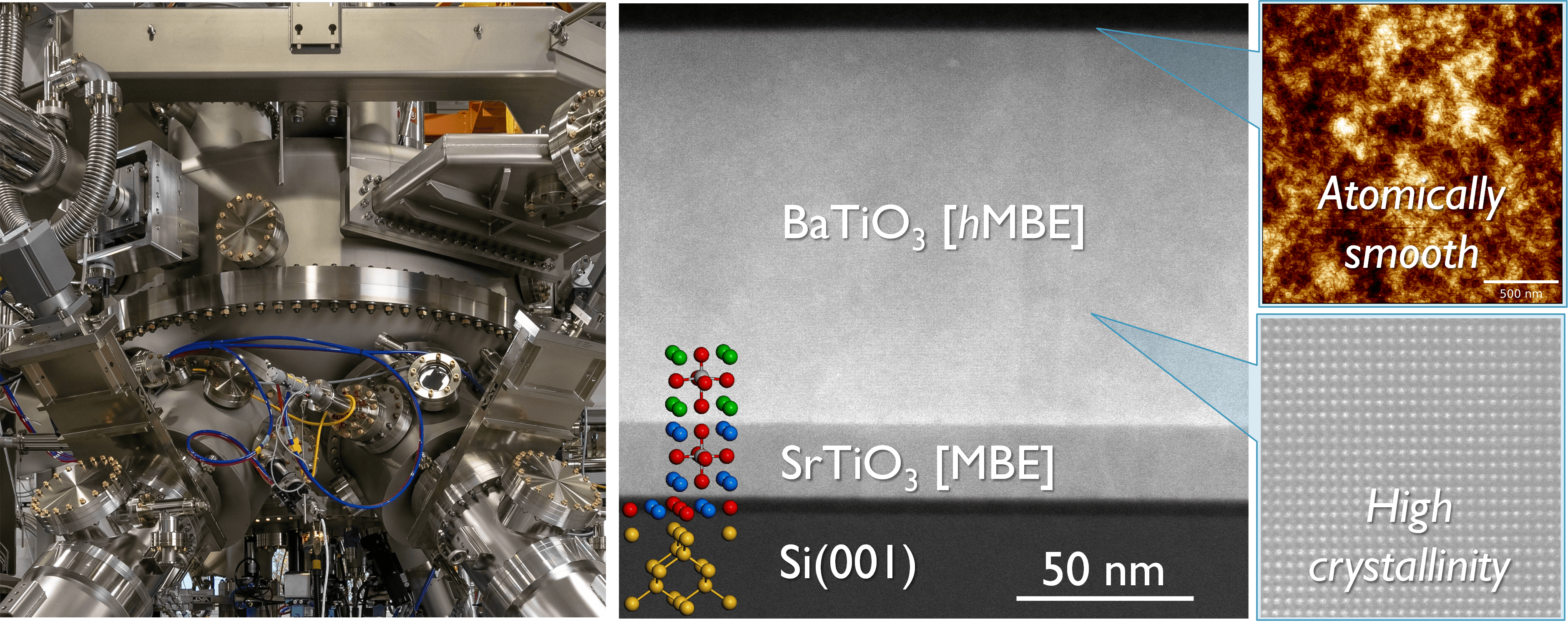
Plainview, N.Y. (U.S.A) and Leuven (Belgium), January 27, 2026 – Veeco Instruments Inc. (Nasdaq: VECO) and imec announced today that they have collaboratively developed a 300mm high-volume-manufacturing-compatible process that enables the integration of barium titanate (BaTiO3 or BTO) on a silicon photonics platform. BTO is a promising material with unique electro-optical properties that can be used for high-speed and low-power light modulation in emerging applications such as high-speed optical transceivers, quantum computing, light detection and ranging (lidar), and AR/VR applications. Historically, approaches to integrate BTO have struggled to meet the desired cost targets to make it viable for high-volume manufacturing. Veeco has now delivered its first molecular beam epitaxy (MBE)-based cluster system, marking a significant milestone in Veeco’s and imec’s partnership and their dedication to enhance silicon photonics platform capabilities. The new 300mm platform is designed for the epitaxy of BaTiO3 single crystalline thin films on silicon, available with both solid and hybrid molecular beam epitaxy (MBE) solutions. With the integration of these alternative growth techniques, the system will be capable of BTO-on-Si deposition with improved repeatability and at a lower cost than classical MBE methods.
The optical transceiver market for datacom is expected to grow to $13.1 billion in 2030, up from $2.9 billion in 2024. However, to alleviate the trade-offs of current silicon modulator technologies, including high power consumption, performance (speed, drive voltage), and area, the introduction of novel electro-optic materials, like BTO, into silicon photonics will be crucial. At present, there is no commercially available production-compatible solution for manufacturing these materials. In partnership with Veeco, imec is now addressing this industry need to develop scaled solutions that allow the integration of materials such as BaTiO3 and SrTiO3 onto a 300mm silicon platform.
“Over the past 4 years, imec and Veeco have collaborated on developing alternative techniques for BaTiO3-on-Si and benchmarking both material and electro-optic properties towards defining a strategy for advancing large-scale manufacturing solutions,” says Clement Merckling, scientific director at imec. “With the introduction of Veeco’s first-of-its-kind MBE solution, we are expanding our capabilities for heterogeneous integration of beyond-Si electro-optic materials, strengthening our R&D offering for current and new partners with an interest in exploring and prototyping next-generation silicon photonics technology.” added Joris Van Campenhout, imec fellow and optical I/O program director.
“This partnership with imec is a monumental step forward for the MBE industry, datacom and quantum computing production,” commented Matthew Marek, Senior Director of Marketing for Veeco’s MBE Product Line. “The historic view of MBE processing has been that it is slow and expensive; however, new hardware developments that our team validated in partnership with imec bring MBE into a cost-effective domain that is suitable for semiconductor fabs. We are excited about the work underway between our two organizations to demonstrate a repeatable, high-volume BTO production process. We anticipate this effort will help us achieve our shared goal to unlock BTO photonic modulator breakthroughs for a better and greener future.”
About Veeco
Veeco (NASDAQ: VECO) is an innovative manufacturer of semiconductor process equipment. Its laser annealing, ion beam, chemical vapor deposition (CVD), metal organic chemical vapor deposition (MOCVD), single wafer etch & clean and lithography technologies play an integral role in the fabrication and packaging of advanced semiconductor devices. With equipment designed to optimize performance, yield and cost of ownership, Veeco holds leading technology positions in the markets it serves. To learn more about Veeco’s systems and service offerings, visit www.veeco.com.
To the extent that this news release discusses expectations or otherwise makes statements about the future, such statements are forward-looking and are subject to a number of risks and uncertainties that could cause actual results to differ materially from the statements made. These factors include the risks discussed in the Business Description and Management's Discussion and Analysis sections of Veeco's Annual Report on Form 10-K for the year ended December 31, 2023 and in our subsequent quarterly reports on Form 10-Q, current reports on Form 8-K and press releases. Veeco does not undertake any obligation to update any forward-looking statements to reflect future events or circumstances after the date of such statements.
About imec
Imec is a world-leading research and innovation hub in advanced semiconductor technologies. Leveraging its state-of-the-art R&D infrastructure and the expertise of over 6,500 employees, imec drives innovation in semiconductor and system scaling, artificial intelligence, silicon photonics, connectivity, and sensing.
Imec’s advanced research powers breakthroughs across a wide range of industries, including computing, health, automotive, energy, infotainment, industry, agrifood, and security. Through IC-Link, imec guides companies through every step of the chip journey - from initial concept to full-scale manufacturing - delivering customized solutions tailored to meet the most advanced design and production needs.
Imec collaborates with global leaders across the semiconductor value chain, as well as with technology companies, start-ups, academia, and research institutions in Flanders and worldwide. Headquartered in Leuven, Belgium, imec has research facilities in Belgium, across Europe and the USA, and representation on three continents. In 2024, imec reported revenues of €1.034 billion.
For more information, visit www.imec-int.com
The imec group holds a global trademark portfolio, including word marks and combined figurative registered and unregistered trademarks, across national, regional, and international territories. Its lawful use requires prior written consent of IMEC in compliance with the IMEC branding guidelines, which may be updated periodically. The latest version is available upon written request.
Discover more
A double world-first: integrating lithium niobate and lithium tantalate modulators on silicon photonics through micro-transfer printing
Read more

Imec demonstrates the co-integration of its high-quality SiN waveguide technology with its active silicon photonics platform
Read more
Imec researchers at Ghent University and Nokia Bell Labs work to debut key building block for the deployment of 100G PON networks
Read more
Design and integration of photonic and electronic integrated circuits for high-speed wireline transceivers
Read more