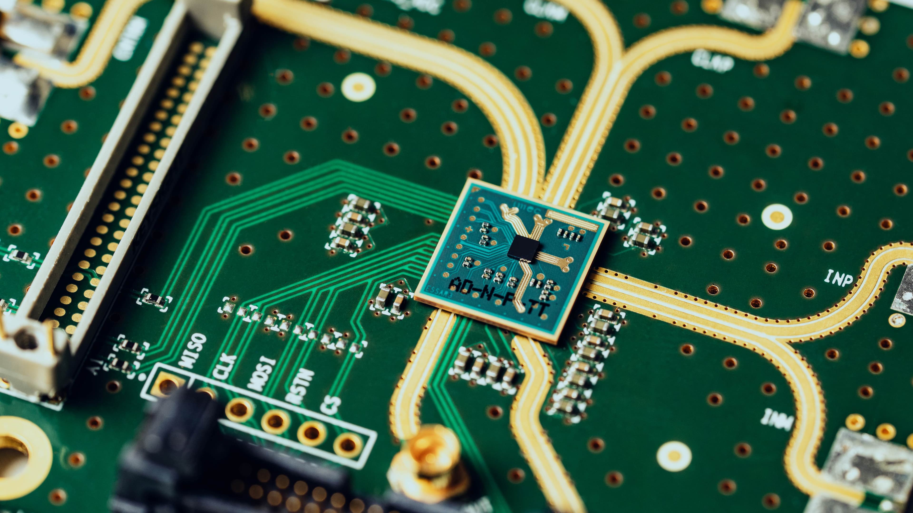
Imec researchers at Ghent University and Nokia Bell Labs work to debut key building block for the deployment of 100G PON networks
Presenting the world’s first upstream 100 Gbit/s PAM-4 linear burst-mode transimpedance amplifier (TIA) chip for the roll-out of next-generation flexible PONs
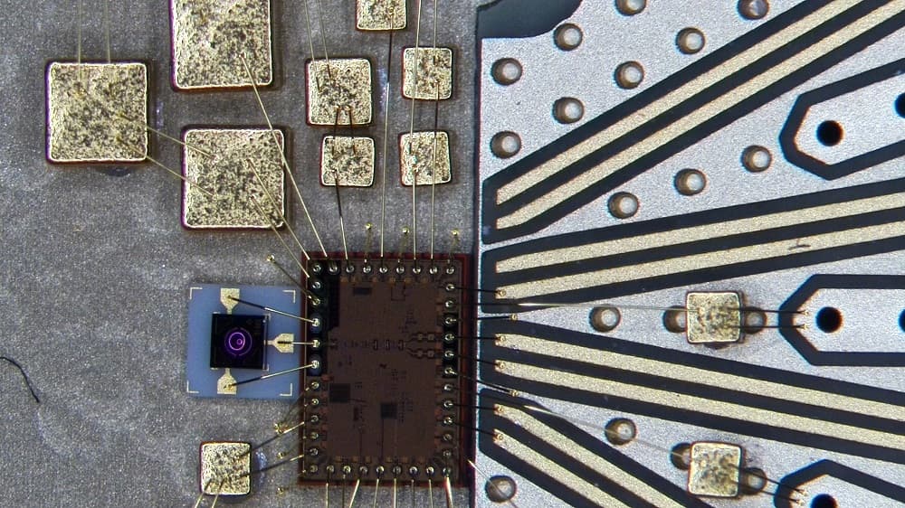
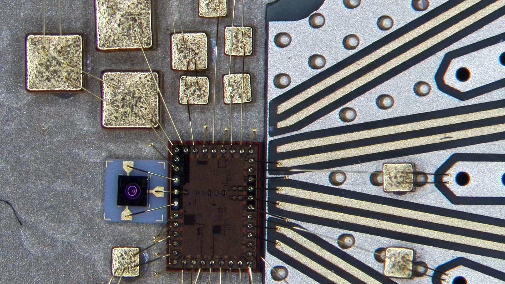
LEUVEN (Belgium), SEPTEMBER 22, 2022 — At this week’s European Conference on Optical Communication (ECOC), researchers from IDLab (an imec research group at Ghent University and the University of Antwerp, Belgium) and Nokia Bell Labs presented the first upstream linear burst-mode transimpedance amplifier (TIA) chip that accommodates 50 Gbit/s NRZ and 100 Gbit/s PAM-4 modulation. The chip enables optical line terminals (OLTs) to cope with upstream packets’ varying signal strength and quality degradation; effects that are compounded by the very high speeds at which next-generation passive optical networks (PONs) operate. This novel TIA chip will be critical to making next-gen flexible PON deployments (and 100G PON networks in particular) technically and economically viable.
Passive optical network (PON) technology brings high-speed broadband to residential and business subscribers, while supporting services such as (5G) mobile fronthaul/backhaul.
PON networks are characterized by a tree-like network topology that allows to serve multiple customers with a common strand of fiber connected to a single optical line terminal (OLT) in the operator’s central office. This makes for a cost-effective deployment scenario, but it also impacts how packets travel the network: downstream traffic is sent over the network continuously, while upstream traffic is transmitted in bursts (within allocated time slots, preventing collisions).
With 10G PON sales skyrocketing and the first 25G PON solutions being commercially introduced, PON technology is evolving rapidly. Still, especially in the upstream direction, several challenges remain to be addressed before next-gen (50G and 100G) PONs can be rolled out.
Optimizing upstream packets’ signal strength quickly and dynamically
Upstream packets arriving at an OLT’s receiver may exhibit a large dynamic range of optical powers. This is due to the differential path loss of the optical distribution network, as well as the variation in optical network terminal (ONT) transmitters’ launch powers. Secondly, the distance between an OLT and its ONTs is a determining factor too (ranging anywhere between a few hundreds of meters, up to a few tens of kilometers).
“As those effects are compounded even further by the high speeds at which next-gen PONs operate, it will be crucial to make sure that all packets arriving at the OLT end up having roughly the same signal strength. Moreover, this must be done with minimal overhead – i.e. no more than a few tens of nanoseconds,” says Gertjan Coudyzer, senior researcher in analog/mixed signal IC design at IDLab, an imec research group at Ghent University and the University of Antwerp (Belgium). “Our novel chip does exactly that, allowing us to use each packet – and the network as a whole – to the fullest, maximizing its speed, reach and throughput.”
Presenting the world’s first upstream linear burst-mode TIA chip, accommodating 50 Gbit/s NRZ and 100 Gbit/s PAM-4 modulation
Gertjan Coudyzer: “During our experiments, we have been able to validate the chip’s linear burst-mode operation; a linearity not only enabling signal equalization, but also paving the way for PAM-4 as a future PON modulation format – doubling the bitrate compared to the use of NRZ. This world’s first is a breakthrough to facilitate the future roll-out of large-scale 100G PONs.”
“Rolling out a fiber network is a huge investment. Once it has been deployed, operators want to leave their network untouched for at least a couple of decades. Today’s announcement confirms that operators’ networks are future-ready, and capable of supporting higher bandwidths should the need for that arise,” adds Peter Ossieur, program manager high-speed transceivers at IDLab. “Going forward, we are looking at the ITU-T to pick up our development and include it in their standardization efforts.”
“The demonstration of our burst-mode transimpedance amplifier chip, resulting from fruitful and long-standing collaboration with imec, re-confirms Nokia’s technical leadership in higher speed passive optical networks,” stated Tod Sizer, Optical System and Device Lab Leader, Nokia Bell Labs. “The results are timely, as targets for 50G upstream PON are being defined in ITU G.9804. Thanks to its linearity, the TIA chip also supports 100G flexrate PON using higher order modulation.”
The TIA chip is fabricated in a 0.13 μm SiGe process. It comes with a power consumption of 275 mW (on average) from a 2.5 V supply. Its total settling time is well under 150 ns, meeting the typical PON target preamble time.
The ever-growing distance between end users and the central office
“Future challenges will continue to be closely linked to the (growing) distance between end users and the central office – as telecom operators try to expand their customer base to more rural areas. Hence, strategies to flexibly provide different customers with different PON flavors from the same OLT will continue to gain momentum, requiring new digital signal processing approaches, updates to the optical receivers, and the development of increasingly linear circuits. Those are exactly the topics that rank highly on our research agenda; topics on which we continue to welcome the input and involvement of partners,” Peter Ossieur concludes.
This work is supported by the VLAIO project SPIC (HBC.2020.2197).

About imec
Imec is a world-leading research and innovation center in nanoelectronics and digital technologies. Imec leverages its state-of-the-art R&D infrastructure and its team of more than 5,000 employees and top researchers, for R&D in advanced semiconductor and system scaling, silicon photonics, artificial intelligence, beyond 5G communications and sensing technologies, and in application domains such as health and life sciences, mobility, industry 4.0, agrofood, smart cities, sustainable energy, education, … Imec unites world-industry leaders across the semiconductor value chain, Flanders-based and international tech, pharma, medical and ICT companies, start-ups, and academia and knowledge centers. Imec is headquartered in Leuven (Belgium), and has research sites across Belgium, in the Netherlands and the USA, and offices in China, India, Taiwan and Japan. In 2021, imec's revenue (P&L) totaled 732 million euro.
Further information on imec can be found at www.imec-int.com.
Imec is a registered trademark for the activities of imec International (IMEC International, a legal entity set up under Belgian law as a “stichting van openbaar nut”), imec Belgium (IMEC vzw supported by the Flemish Government), imec the Netherlands (Stichting IMEC Nederland), imec Taiwan (IMEC Taiwan Co.), imec China (IMEC Microelectronics (Shanghai) Co. Ltd.), imec India (IMEC India Private Limited), imec San Francisco (IMEC Inc.) and imec Florida (IMEC USA Nanoelectronics Design Center Inc.).
Discover more

Veeco and imec develop 300mm-compatible process to enable integration of barium titanate on silicon photonics
Read more
A double world-first: integrating lithium niobate and lithium tantalate modulators on silicon photonics through micro-transfer printing
Read more
Disruptive ‘Wi-Fi on steroids’ technology allows manufacturing industry to finally cut the cord
Read more
Advanced semiconductor packaging approach from AT&S and imec lays the foundation for compact, cost-efficient, and high-performance 140 GHz radar & 6G mobile communications systems
Read more