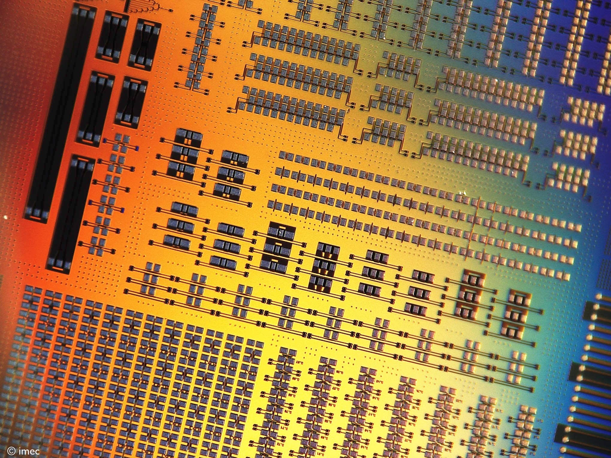
A double world-first: integrating lithium niobate and lithium tantalate modulators on silicon photonics through micro-transfer printing
Breakthroughs in heterogeneous photonic integration are charting a path toward future, scalable data center interconnects
In short
Researchers from imec and Ghent University have successfully transfer-printed thin-film lithium niobate modulators onto imec’s silicon photonics platform – an industry first.
In parallel, they were the first to heterogeneously integrate a lithium tantalate modulator on a silicon photonic integrated circuit (PIC).
The researchers view these breakthroughs as key milestones in heterogeneous photonic integration, demonstrating the potential to seamlessly integrate emerging materials through micro-transfer printing – thus setting the stage for the next generations of optical interconnects.
Hear Bart Kuyken break down the team’s latest Nature Photonics work in the video interview at the end of this article - from materials, and integration, to the future impact of micro-transfer printing on scaling data center interconnects and enabling a host of quantum applications. Courtesy: All Things Photonics.
The popularity of cloud computing and AI – driving massive data flows – pushes demand for ultra-high-speed, energy-efficient optical links within and between data centers; links that must be able to deliver data rates well beyond today’s 200Gb/s standard. The heterogeneous integration of new materials onto silicon photonics platforms will enable next-gen electro-optical modulators and detectors for such short-reach and short-haul interconnects.
One standout material is lithium niobate (LiNbO3), renowned for its high electro-optic coefficient, making it an excellent fit for high-speed optical communication systems. Another contender is lithium tantalate (LiTaO3), valued for its electro-optic stability, high damage threshold, and UV transparency – qualities that make it ideal for high-power, temperature-sensitive applications, and systems operating at shorter wavelengths.
However, both materials contain lithium, which complicates their compatibility with standard CMOS fabrication processes. And integrating other components, such as high-speed photodetectors, alongside these materials is also far from trivial.
To address these challenges, various integration approaches are being explored. Wafer bonding, for instance, has been demonstrated with lithium niobate, but it remains costly and inefficient – since most of the material must be removed after bonding and many additional post-bonding processing steps are needed. Today, imec introduces micro-transfer printing as a promising alternative for heterogeneously integrating LiNbO3 and LiTaO3 onto a silicon photonics platform.
World first: integrating thin-film LiNbO3 modulators on a silicon photonics platform using micro-transfer printing
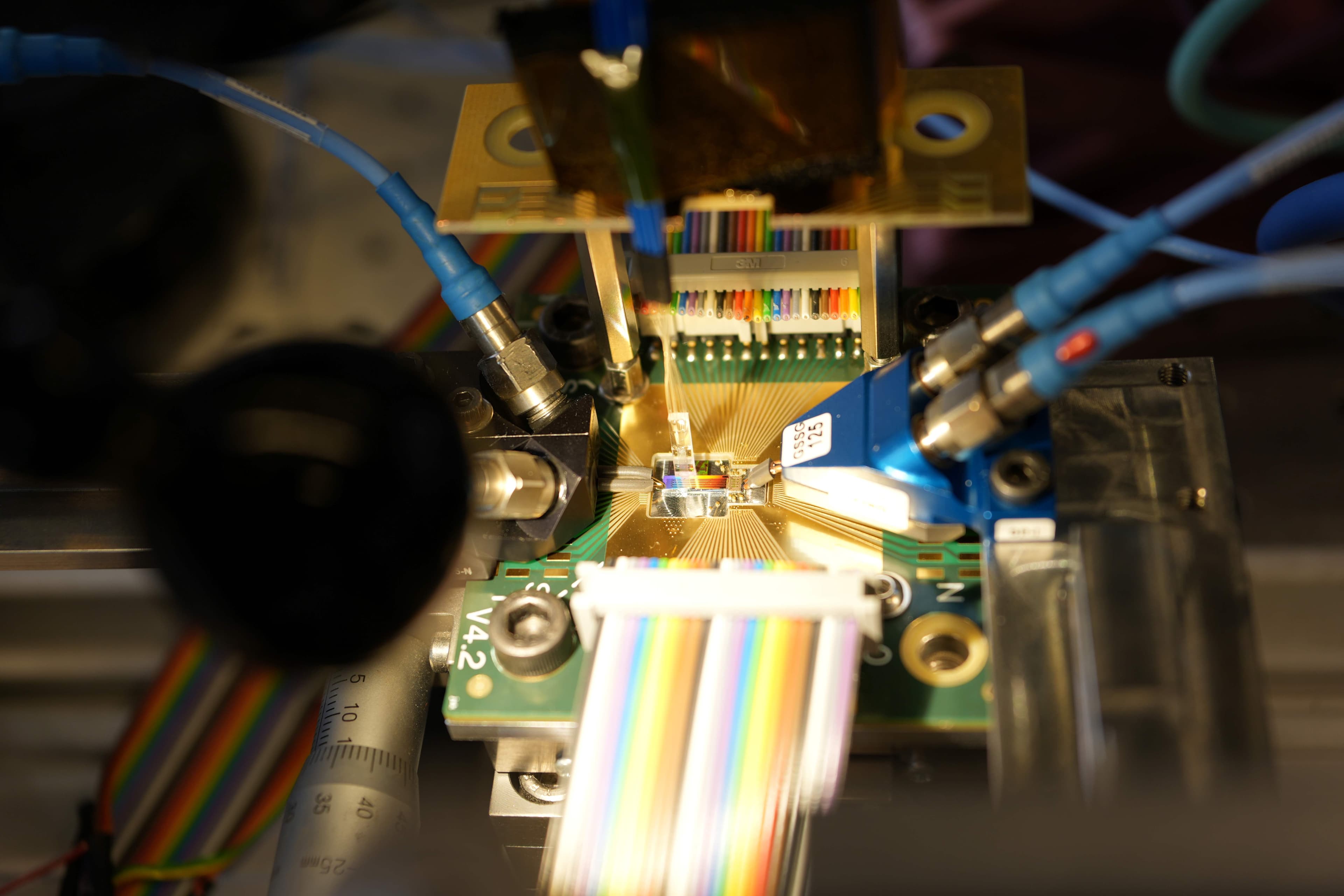
At this year’s European Conference on Optical Communication (ECOC), researchers from imec and Ghent University showcased an O-band 320Gb/s unamplified optical link over 2 km of standard single-mode fiber, utilizing novel high-speed integrated circuits that are fully compatible with standard CMOS manufacturing. [1]
A world first, the proof of concept leverages a high-bandwidth 100GHz germanium photodiode and transfer-printed thin-film lithium niobate Mach-Zehnder modulators (MZMs) onto imec’s silicon photonics platform, co-packaged with custom-designed traveling-wave drivers and transimpedance amplifiers (TIAs).

This breakthrough makes imec the first to achieve the seamless integration of thin-film LiNbO3 devices on silicon photonics. The team’s work involved adapting and refining the proper SiPh process flows, as well as co-developing photonic and electronic integrated circuits (PICs and EICs) for maximum performance. The resulting proof of concept suggests a path toward optical interconnects delivering 400Gb/s per lane.
First-ever integration of a thin-film LiTaO3 modulator on silicon photonics
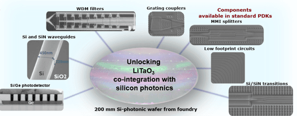
In another pioneering achievement, described in a recent article in Nature Photonics, the first heterogeneous integration of a LiTaO3 modulator on a silicon photonic integrated circuit was demonstrated. [2]
Using the same micro-transfer printing technique previously applied to lithium niobate, the approach ensures full compatibility with the entire wafer stack. It enables seamless co-integration with other components such as heaters, filters, and germanium photodetectors – without compromising their performance.
“Building on our work with lithium niobate, we found that the same micro-transfer printing technique can be applied to lithium tantalate as well, demonstrating its exceptional versatility,” commented Margot Niels, the research paper’s first author. “This gives us strong confidence that, as new materials emerge, we will be able to integrate them just as effectively on silicon photonics – thus laying the groundwork for the next generations of optical interconnects.”
Enabling the race toward the 400Gb/s optical interconnect milestone
These research results exemplify imec’s ambition to push the boundaries of high-speed optical and electronic circuit design. Although significant work remains before the approach can be fully matured for commercial adoption, exploring new materials and integrating these advances into next-generation proofs of concept is a crucial step in the race toward the 400Gb/s optical interconnect milestone.
This work was conducted under the guidance and support of Bart Kuyken, Maximilien Billet and Tom Vanackere from imec's Photonics Research Group at Ghent University, and Xin Yin (Scott), Nishant Singh and Cedric Bruynsteen (now with NVidia) from IDLab, an imec research group at Ghent University.
Want to know more?
- [1] Declercq, J. et al., "320 Gb/s Unamplified Transmission Using 1 00 GHz Ge PD and TFLN MZM on a Foundry-Compatible SiPh Platform Co-Packaged with Traveling-Wave Drivers and TIAs," 2025 European Conference on Optical Communications (ECOC), Copenhagen, Denmark, 2025, pp. 1-4, doi: 10.1109/ECOC66593.2025.11263113.
- [2] Niels, M., Vanackere, T., Vissers, E. et al., "A High-Speed Heterogeneous Lithium Tantalate Silicon Photonics Platform," Nat. Photon. 20, 225–231 (2026). https://doi.org/10.1038/s41566-025-01832-9, in Nature Photonics.
Authors

Margot Niels
Margot Niels received her BSc and MSc degrees in Electronics and ICT Engineering Technology from Ghent University, Belgium, in 2019 and 2020, respectively. She then earned an additional MSc in Electrical Engineering from Ghent University in 2022. During her thesis work on a silicon photonic Butler matrix, Margot collaborated with imec’s Photonics Research Group at Ghent University, sparking her interest in photonics.
In September 2022, she joined the Photonics Research Group as a PhD student, where she is currently finalising her work on developing a wafer-scale micro-transfer printing technique to heterogeneously integrate lithium niobate on a silicon photonic platform

Jakob Declercq
Jakob Declercq was born in Kortrijk, Belgium in 1997. He obtained his Bachelor of Science in Engineering and Master of Science in Electrical Engineering from Ghent University, Belgium, in 2018 and 2020 respectively. He recently earned his Ph.D. at Ghent University, where he is affiliated with IDLab, an imec research group at Ghent University. His current research interests focus on opto-electronic transceiver chip design for high-speed broadband IMDD and coherent optical communication systems.
Discover more


Veeco and imec develop 300mm-compatible process to enable integration of barium titanate on silicon photonics
Read more
Imec demonstrates the co-integration of its high-quality SiN waveguide technology with its active silicon photonics platform
Read more
Imec unveils 7‑bit, 175GS/s massively time-interleaved slope-ADC – pairing record-small footprint and low conversion energy with top sampling speed
Read more