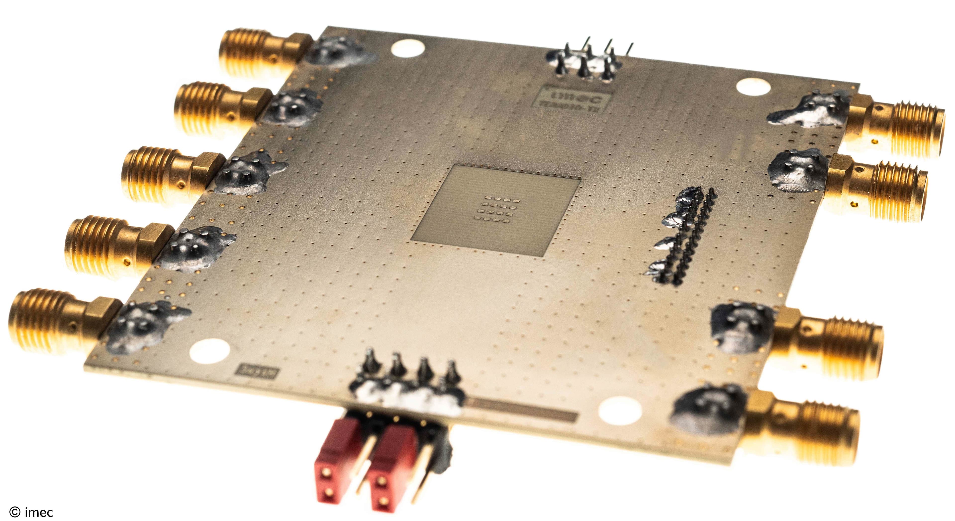
Imec achieves record-breaking RF GaN-on-Si transistor performance for high-efficiency 6G power amplifiers
Improved contact resistance and RF output key toward mobile-compatible E-mode GaN-on-Si transistors

LEUVEN (Belgium), June 12, 2025— Imec, a world-leading research and innovation hub in nanoelectronics and digital technologies, has set a new benchmark in RF transistor performance for mobile applications. They present a gallium nitride (GaN) MOSHEMT (metal-oxide-semiconductor high-electron-mobility transistor) on silicon (Si) that achieves both record efficiency and output power for an enhancement-mode (E-mode) device operating at low supply voltage. In parallel, imec also demonstrated a record-low contact resistance of 0.024Ω· mm which is essential to further boost output power in future designs. The results mark a crucial step toward integrating GaN technology into next-gen mobile devices, particularly those targeting the 6G FR3 band between 7 and 24GHz. The results will be presented at the 2025 Symposium on VLSI Technology and Circuits in Kyoto, Japan.
Today’s mobile networks largely operate below 6GHz, but to meet the data rate demands of future 6G systems, a shift to higher frequencies is needed. In these bands, current mobile solutions based on gallium arsenide (GaAs) HBTs (heterojunction bipolar transistor) struggle to maintain performance. Their efficiency and gain degrade significantly above 10 to 15GHz, leading to fast battery drain and poor energy use in user equipment. GaN is widely recognized as a promising alternative because of its higher power density and breakdown voltage. While GaN transistors on silicon carbide (SiC) have shown strong RF performance in high-frequency base station applications, the cost and limited wafer scalability of SiC remain barriers for the mobile market.
Silicon is a more scalable and cost-effective platform but building high-efficiency GaN transistors on it has been challenging due to the lattice and thermal mismatch between the two materials, which can compromise material quality and device reliability. The challenge is even greater for E-mode designs –which are preferred in mobile for their fail-safe operation and low power consumption – because it typically requires thinning the transistor barrier and channel under the gate. This limits the on-current and increases the off-state leakage, making it harder to achieve the power, efficiency, and gain needed for 6G.
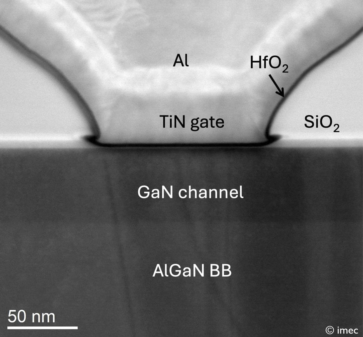
Imec now demonstrates a GaN-on-Si E-mode MOSHEMT that reaches a record 27.8dBm (1W/mm). output power and 66% power-added efficiency (PAE) at 13GHz and 5V. The result was obtained in a single device with an 8-finger gate layout, providing the gate width needed for high output power without requiring the combined power of multiple transistors. The excellent performance was enabled by combining a gate recess technique, used to shift the device into E-mode, with an InAlN barrier layer that offsets the performance loss from the thinned channel.
In parallel to the device development, imec demonstrated a record-low contact resistance of 0.024Ω· mm using a regrown n⁺(In)GaN layer maximizing current flow and minimizing power loss. While the result was obtained in a separate module, it is fully compatible with the E-mode transistor architecture. Simulations indicate that integrating this contact module could improve the output power density by 70%, meeting the performance target for 6G user equipment.
“Reducing contact resistance is crucial for pushing output power while keeping efficiency high,” said Alireza Alian, Principal Member of Technical Staff at imec. “Our next step is to integrate this contact module into the E-mode transistor and validate the expected gains in power and efficiency, bringing the device closer to real-world 6G applications.”
About imec
Imec is a world-leading research and innovation center in nanoelectronics and digital technologies. Imec leverages its state-of-the-art R&D infrastructure and its team of more than 6.000 employees and top researchers, for R&D in advanced semiconductor and system scaling, silicon photonics, artificial intelligence, beyond 5G communications and sensing technologies, and in application domains such as health and life sciences, mobility, industry 4.0, agrofood, smart cities, sustainable energy, education, … Imec unites world-industry leaders across the semiconductor value chain, Flanders-based and international tech, pharma, medical and ICT companies, start-ups, and academia and knowledge centers. Imec is headquartered in Leuven (Belgium), and has research sites across Belgium, in the Netherlands, the UK and the USA, and representation in 3 continents. In 2024, imec's revenue (P&L) totaled 1,034 billion euro.
Further information on imec can be found at www.imec-int.com.
The imec group holds a global trademark portfolio, including word marks and combined figurative registered and unregistered trademarks, across national, regional, and international territories. Its lawful use requires prior written consent of IMEC in compliance with the IMEC branding guidelines, which may be updated periodically. The latest version is available upon written request.
Discover more

Imec unlocks system-level III-V chiplet integration on Si-CMOS by advancing its 300mm RF silicon interposer platform with high-density MIMCAPs, passive modeling, and laser-assisted bonding
Read more
Imec presents 150 GSa/s Digital-to-Analog Converter (DAC) achieving 300 Gb/s data transmission
Read more
Imec and Ghent University present a fully-integrated, single-chip microwave photonics system for compact and versatile signal processing
Read more
300mm RF silicon interposer platform for chiplet-based heterogeneous integration demonstrates record-low insertion loss at frequencies up to 325GHz
Read more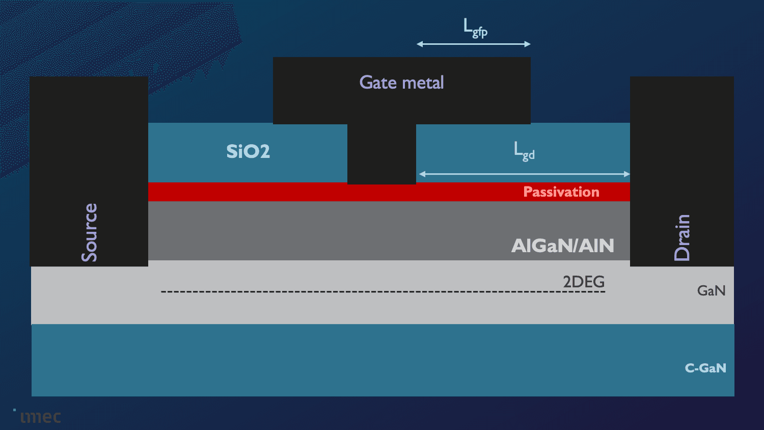
Imec achieves seamless InP Chiplet integration on 300mm RF Silicon Interposer with excellent performance at 140GHz
Read more
Imec introduces best-in-class ADCs for base stations and smartphones, propelling beyond-5G communications
Read more