300mm RF silicon interposer platform for chiplet-based heterogeneous integration demonstrates record-low insertion loss at frequencies up to 325GHz
Flexible integration of digital, analog, RF-to-sub-THz CMOS and III/V chiplets on a single carrier paves the way for high-performance RF and mixed-signal applications
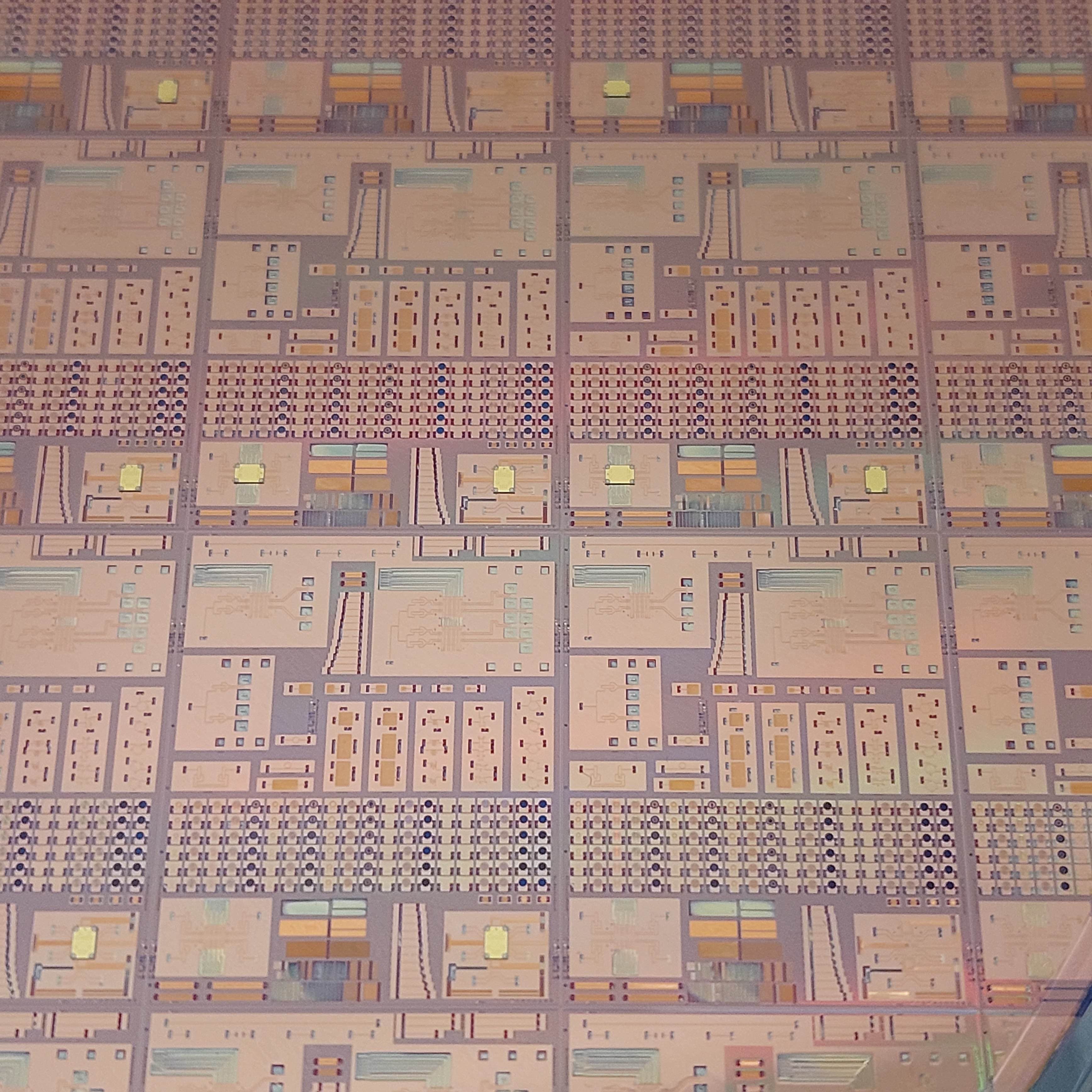
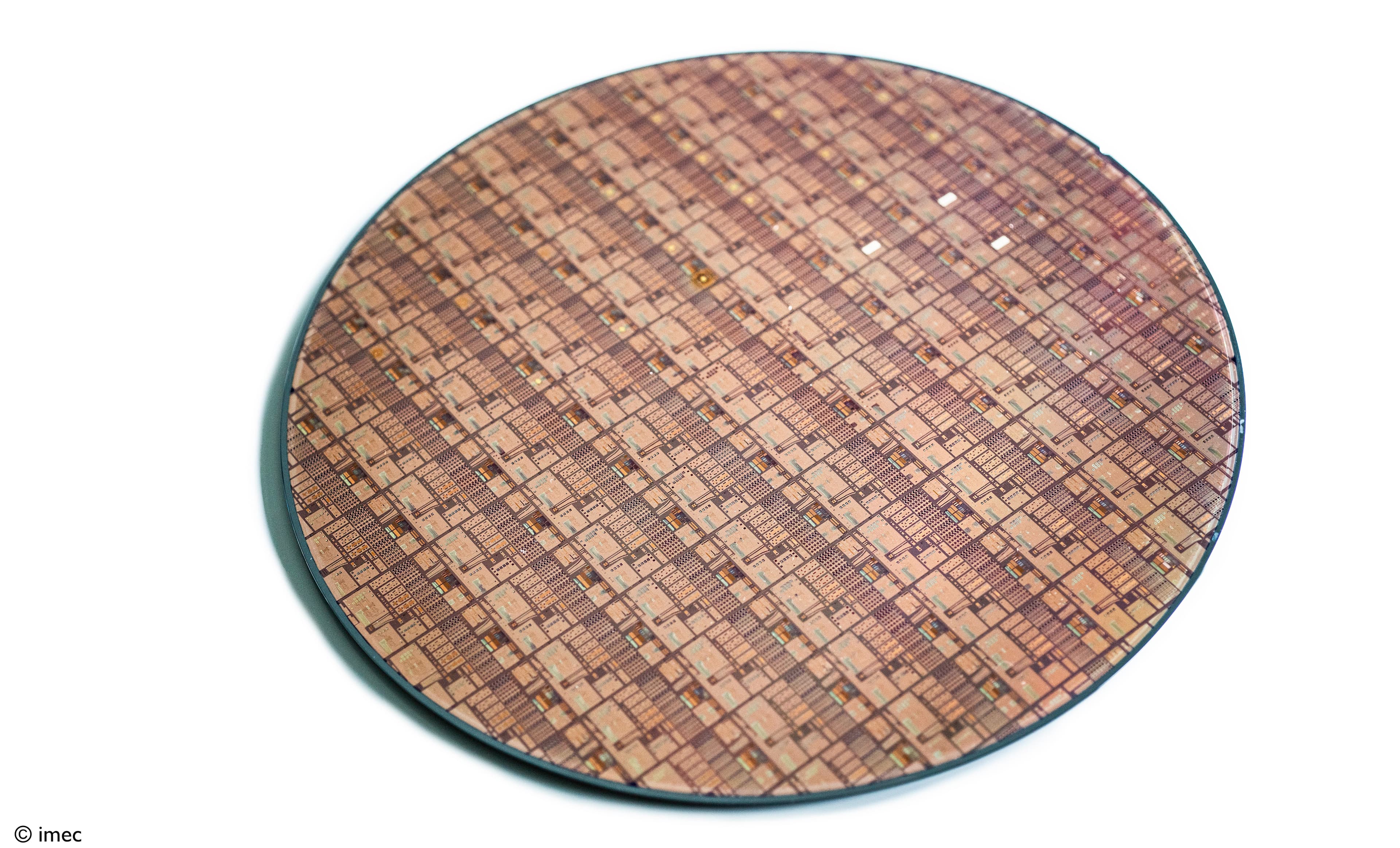
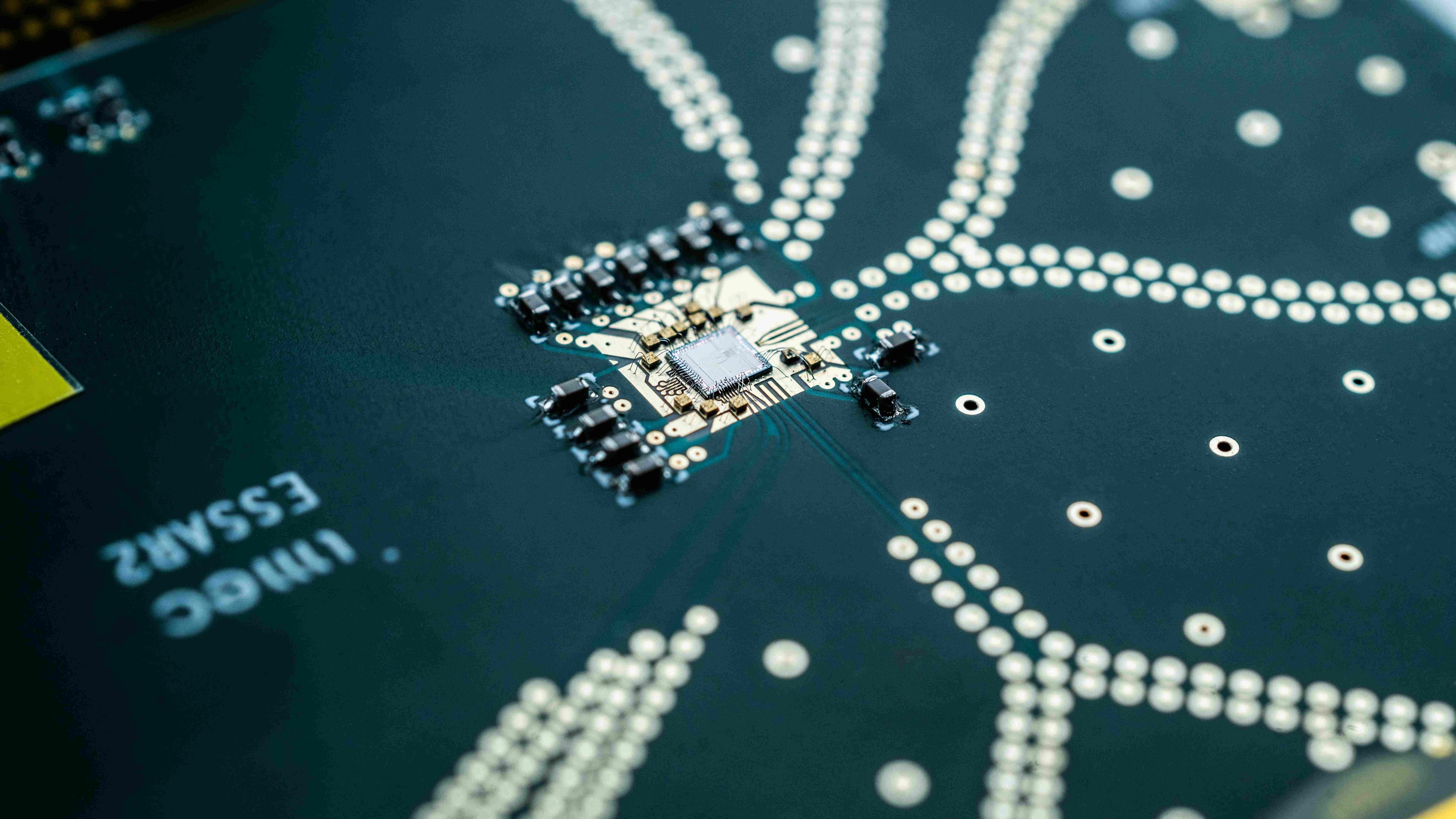
LEUVEN (Belgium), MAY 27, 2025 — At the IEEE ECTC 2025 conference, imec – a world-leading research and innovation hub in nanoelectronics and digital technologies – highlights the exceptional performance and flexibility of its 300mm RF silicon interposer platform. The platform enables seamless integration of RF-to-sub-THz CMOS and III/V chiplets on a single carrier, achieving a record-low insertion loss of just 0.73dB/mm at frequencies up to 325GHz. This advancement paves the way for compact, low-loss, and scalable next-generation RF and mixed-signal systems.
In pursuit of advanced applications – from wireless data centers and high-resolution automotive radar to pluggable optical transceivers and ultra-high-speed wireless USB solutions for short-range device-to-device communications – industry momentum is rapidly shifting to mmWave (30-100GHz) and sub-THz (100-300GHz) frequency bands.
However, unlocking the potential of these higher frequencies requires components that combine the high output power and drive capabilities of III/V materials with the scalability and cost-efficiency of CMOS technology – all integrated on a single carrier. This is where chiplet-based heterogeneous systems, built on RF silicon interposer technology, make the difference – enabling the seamless integration of digital and RF components.
A 300mm RF Si interposer with record-low insertion loss of 0.73dB/mm at 325GHz
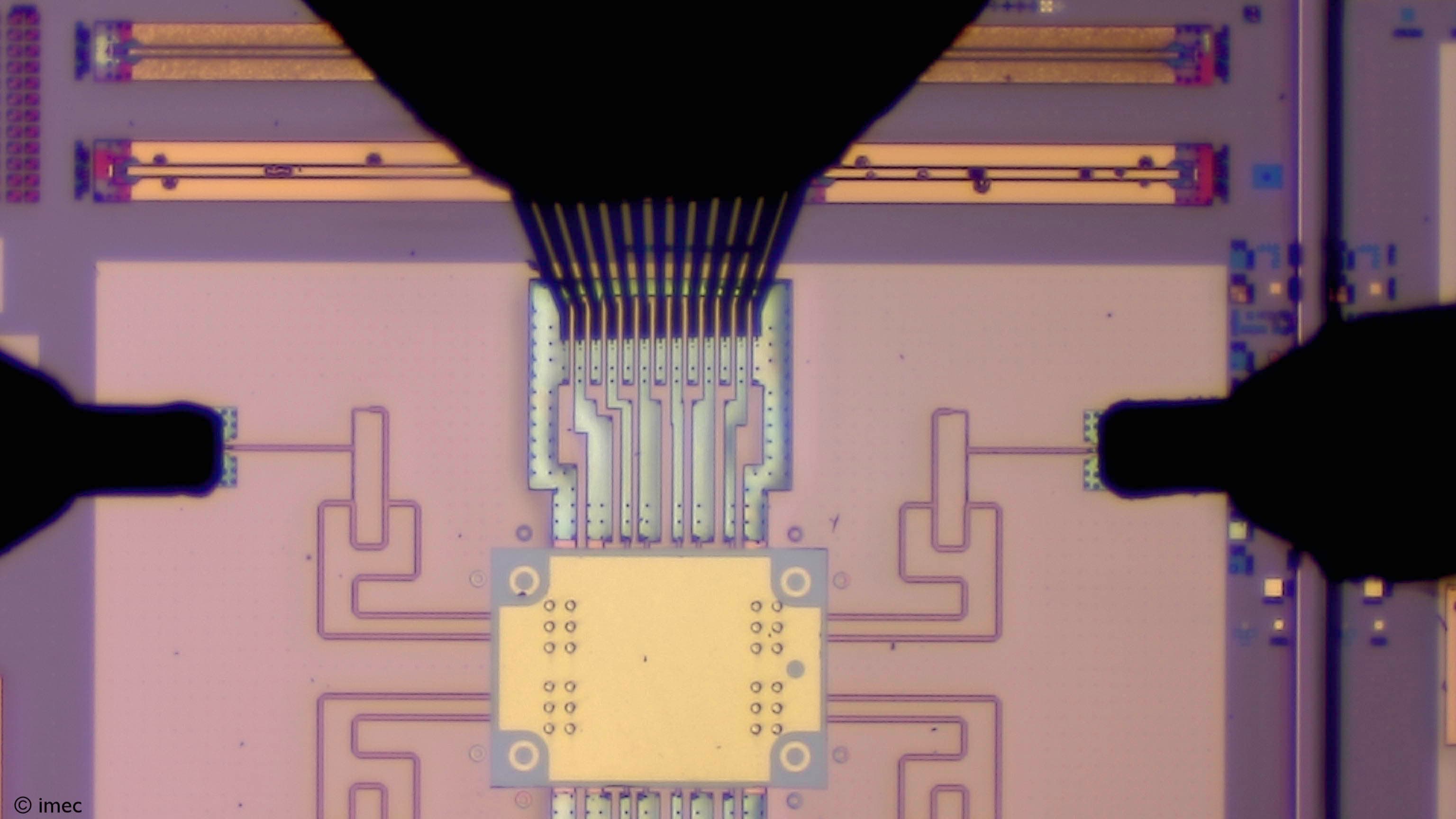
At last year’s IEDM, imec reported a breakthrough in the hetero-integration of InP chiplets on a 300mm RF Si interposer – at frequencies up to 140GHz. Now, at ECTC 2025, imec announces a new milestone: using the same Si interposer platform, it has demonstrated a record-low insertion loss of just 0.73dB/mm at frequencies up to 325GHz.
“What sets our approach apart is the ability to mix and match digital, RF-to-sub-THz CMOS technology nodes with a wide variety of III/V chiplets – not limited to InP, but also including SiGe, GaAs, and others,” said Xiao Sun, principal member of technical staff at imec.
The platform’s digital interconnects benefit from Cu damascene back-end-of-line (BEOL) processing, while mmWave signal paths employ transmission lines on a low-loss RF polymer layer. Additionally, high-quality passive components – such as inductors – are integrated directly onto the RF silicon interposer, reducing the active chip area, lowering costs, and ensuring compact, low-loss RF interconnects for improved performance.
Imec’s technology combines RF/microwave links (with 5µm line width and 5µm spacing), with high-density digital interconnects (with 1µm/1µm line/spacing), and a fine flip-chip pitch of 40µm – with efforts underway to scale down to 20µm. Together, these features enable high integration density and a compact footprint.
The path forward: opening the platform to partners for prototyping
As a next step, Xiao Sun and her team are preparing to augment the platform with additional features – including through-silicon vias, back-side redistribution layers, and MIMCAPs for supply decoupling. In parallel, imec is preparing to open its RF interposer R&D platform to partners for early assessment, system validation, and prototyping – amongst others by evaluating access via NanoIC, imec’s sub-2nm pilot line as part of the EU Chips Act.
These research advancements will be discussed on Tuesday, May 27, from 3:30 PM to 5:00 PM (CST) during the special session “Advancements in mmWave and Sub-THz Packaging for Communication & Radar Applications” at ECTC. A detailed presentation of the results will follow on Wednesday, May 28 at 11:55 AM (CST), during ECTC’s “Session 5: Advanced Design for Heterogeneous Integration”.
About imec
Imec is a world-leading research and innovation center in nanoelectronics and digital technologies. Imec leverages its state-of-the-art R&D infrastructure and its team of more than 6.000 employees and top researchers, for R&D in advanced semiconductor and system scaling, silicon photonics, artificial intelligence, beyond 5G communications and sensing technologies, and in application domains such as health and life sciences, mobility, industry 4.0, agrofood, smart cities, sustainable energy, education, … Imec unites world-industry leaders across the semiconductor value chain, Flanders-based and international tech, pharma, medical and ICT companies, start-ups, and academia and knowledge centers. Imec is headquartered in Leuven (Belgium), and has research sites across Belgium, in the Netherlands, the UK and the USA, and representation in 3 continents. In 2024, imec's revenue (P&L) totaled 1,034 billion euro.
Further information on imec can be found at www.imec-int.com.
The imec group holds a global trademark portfolio, including word marks and combined figurative registered and unregistered trademarks, across national, regional, and international territories. Its lawful use requires prior written consent of IMEC in compliance with the IMEC branding guidelines, which may be updated periodically. The latest version is available upon written request.
Discover more
Imec achieves seamless InP Chiplet integration on 300mm RF Silicon Interposer with excellent performance at 140GHz
Read more
Imec unveils CMOS-based 56Gb/s zero-IF D-band beamforming transmitter, featuring superior output power and energy efficiency
Read more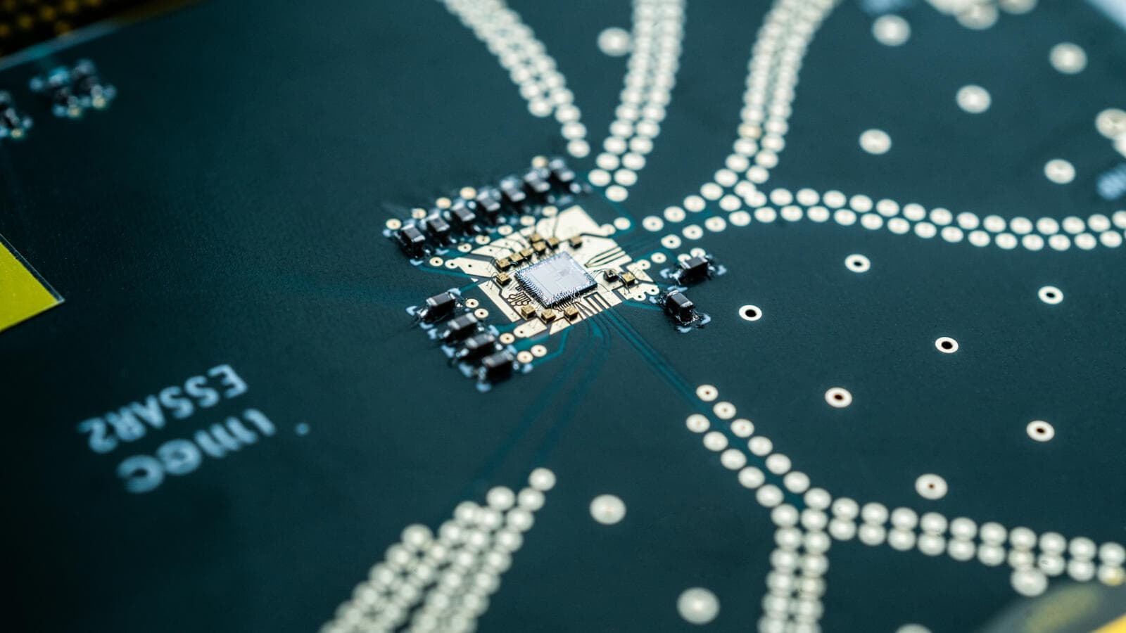
Imec Unveils Breakthrough ADC Architecture for Very High-Speed Wireline Applications, Excelling in Area & Power Efficiency
Read more
Imec unlocks system-level III-V chiplet integration on Si-CMOS by advancing its 300mm RF silicon interposer platform with high-density MIMCAPs, passive modeling, and laser-assisted bonding
Read more
Imec achieves record-breaking RF GaN-on-Si transistor performance for high-efficiency 6G power amplifiers
Read more
Imec presents 150 GSa/s Digital-to-Analog Converter (DAC) achieving 300 Gb/s data transmission
Read more