Back end of line (BEOL) nano-interconnects
To fully reap the benefits of device scaling, the back end of line (BEOL) also needs to evolve. Together with industry leaders, imec is exploring all the options.
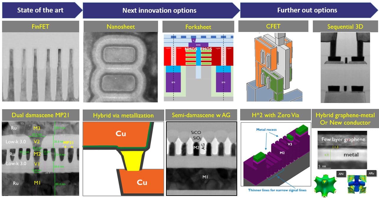
The back end of line (BEOL) is the final state semiconductor processing that concerns the interconnects that reside in the top part of a chip. In today's advanced IC's, that consists of up to fifteen layers of complex wiring. As device scaling continues to 3 nm and beyond, the interconnects will also be affected. This requires new materials and integration schemes, process innovations and scaling boosters. A range of these options are under development in imec’s labs, where the toolbox for the next decade’s interconnects are being enabled.
Mitigating the thermal bottlenecks in advanced interconnects

Do you want regular updates on imec’s semiconductor research?
New BEOL process and integration schemes
The pitches of the deepest, most critical interconnect layers will be reduced to 20 nm and below. This requires disruptive integration schemes such as hybrid metallization, semi-damascene metallization, and hybrid-height-with-zero-via structures combined with new materials.
Of major importance to interconnect and contact processing has been the insertion of single-print extreme ultraviolet (EUV) lithography, a development that imec and its partners have enabled. For the future, we now investigate, amongst others, EUV multipatterning.
Next to the critical layers, imec’s scientists and expertise centers design and assess interconnect schemes from the cell level all the way up to block level.
Scaling boosters
An essential part of BEOL scaling is to enable performance and structural boosters. These will put a turbo on logic IC scaling and will help to make cells smaller. At the same time, the mechanical stability and thermal management remains crucial.
Some of the scaling boosters that imec considers:
- buried power rails
- self-aligned vias
- hybrid-height-with-zero vias
- airgaps
For example: a self-aligned semi-damascene approach combined with high-aspect-ratio, gapfill and airgap is very competitive at cell- and block-level power and delay options.
New materials for the BEOL
Both high-performance and low-power options require conductors with low resistance, better even than for example copper, cobalt or tungsten. Therefore, the race to identify the most promising metallic compounds is on, and imec’s scientists and partners are working to enable exciting material options. Next to metals, we’re also looking at a hybrid graphene/metal conductor, using the exceptional electrical and thermal characteristics of single-layer graphene.
Adding extra functionality to the BEOL
An exciting road would be to integrate thin-film transistors (TFTs) in the BEOL. This of course depends on finding BEOL-compatible materials with a high-enough mobility. At the intermediate level of interconnects, for example beyond layer 6, the density of vias is relatively low. This leaves space for additional BEOL-compatible transistors, which could assume interesting functions such as power management, signal buffering, or one of the longstanding interconnect dreams: repeaters.
Read more
How hyperscalers are rethinking AI infrastructure
To move data faster, farther, and more efficiently, the AI ecosystem is exploring RF silicon interposer technology that allows to heterogeneously integrate CMOS, BiCMOS, and III-V materials
Read more
Optical interconnect research program
Imec’s pre-competitive research program unites material and tool suppliers, foundries, IDMs, OSATs, fabless and system companies in the exploration of future optical interconnect technologies.
Read more
A double world-first: integrating lithium niobate and lithium tantalate modulators on silicon photonics through micro-transfer printing
Breakthroughs in heterogeneous photonic integration are charting a path toward future, scalable data center interconnects
Read more