Advanced patterning and key process steps
Imec and its partners are working on the improved tools and processes that are indispensable for the advancement of consecutive technology nodes.
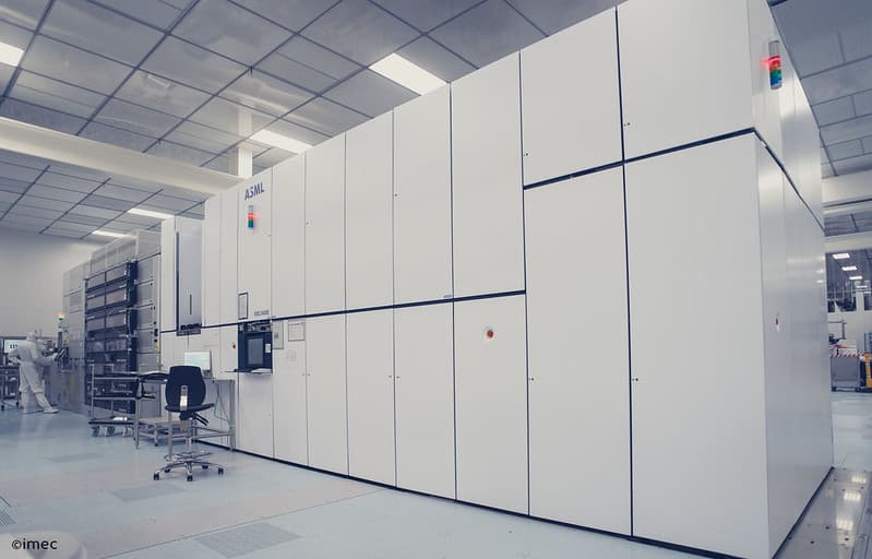
Imec works with the world’s leading equipment and material suppliers to develop the most advanced patterning techniques. We combine:
- advanced imaging
- novel patterning materials
- new etch capabilities
- state-of-the-art metrology
These tools and techniques are available in imec’s advanced 300mm cleanroom, resulting in a unique, vendor-neutral lab where the processes for next-generation logic and memory circuits are developed and perfected.
2026 press release: Imec unlocks lever for EUV dose reduction
Do you want regular updates on imec’s semiconductor research?
Do you develop patterning tools, resist chemicals, semiconductor materials, analysis software, semiconductor process technology tools? Or are you perfecting advanced process steps for next technology nodes? Then you’re sure to benefit from imec’s ecosystem, cleanroom and many collaboration options.
Advanced lithography
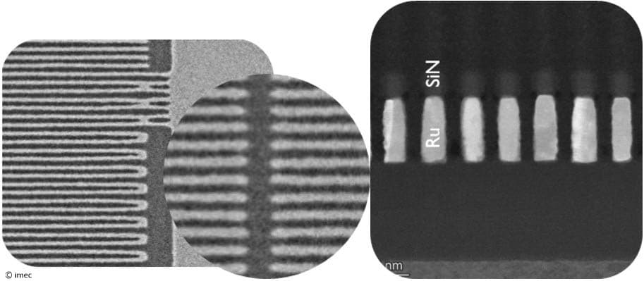
In the frame of the Advanced Patterning Center collaboration with ASML, we’re developing next-generation EUV patterning solutions while accelerating the industrialization of EUV lithography by pro-actively analyzing and solving technical challenges related to stochastic defects, reliability and yield.

To help do that, we’ve set up the AttoLab, where we can image at high-NA EUV dimensions and study EUV photon absorption and subsequent ionization processes at unprecedented timescales from attoseconds to picoseconds.
High NA EUV lithography: launching the industry into the angstrom era
High NA EUV lithography is crucial to extend the logic and memory technology roadmaps into sub-2nm territory.
The case for High NA EUV: unlocking the next era of chip manufacturing
Imec plays a key role in the accelerated adoption of High NA for mass manufacturing. Its pre-competitive research program brings together over 50 partners, from chip manufacturers to equipment/material suppliers and metrology experts sharing risks, costs and IP. They work with imec’s long-time experts on challenges such as mask and imaging optimization, and advanced etch and metrology.
This unmatched access to tools and expertise would be impossible without the unique collaboration between imec and ASML on High NA EUV.
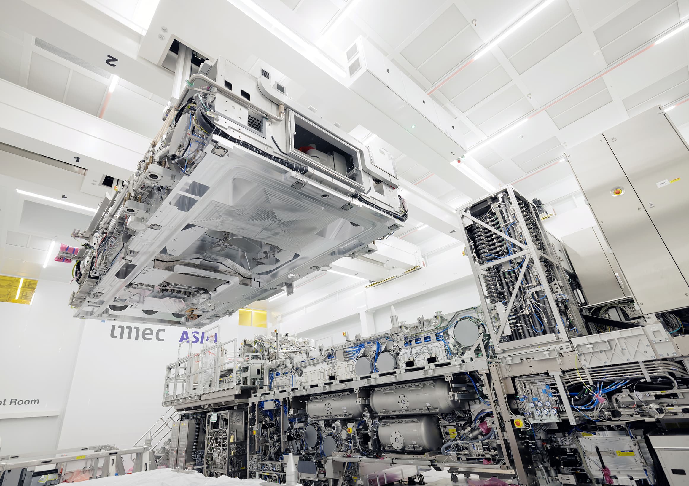
In a first phase, this resulted in a joint High NA lab built around the TWINSCAN EXE:5000.
In the next phase, these activities are ramped up on the next-generation TWINSCAN EXE:5200. This latest High NA tool was installed in March 2026 as part of the imec pilot line in Leuven, supported by the European NanoIC project.
Want to join our research?
Click the button below to get in touch.
Read more
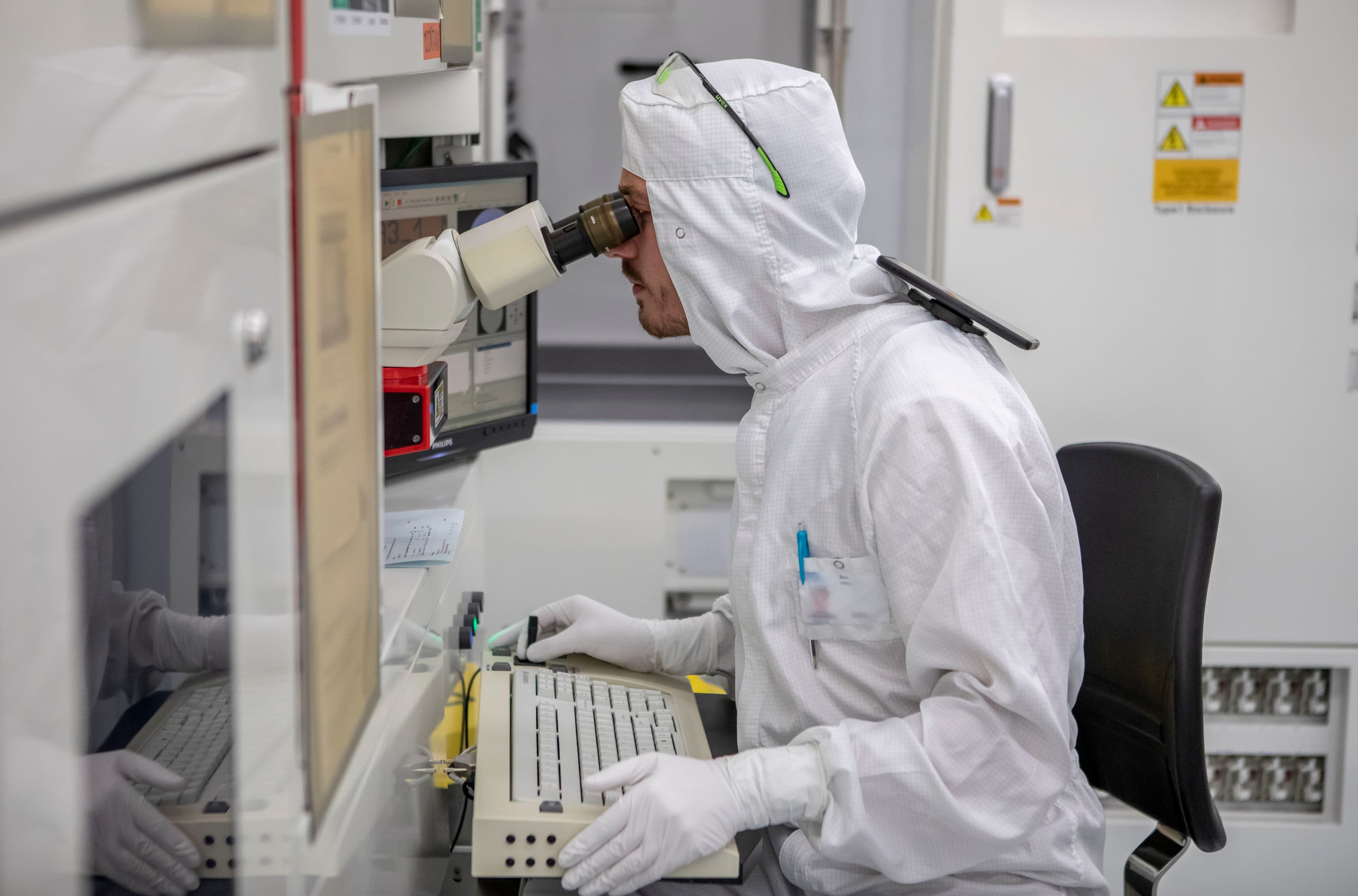
Four decades of in-fab metrology and inspection: pivotal milestones, and the road ahead
Linking advances in in-fab metrology and inspection to critical periods in the patterning and logic device roadmap
Read more
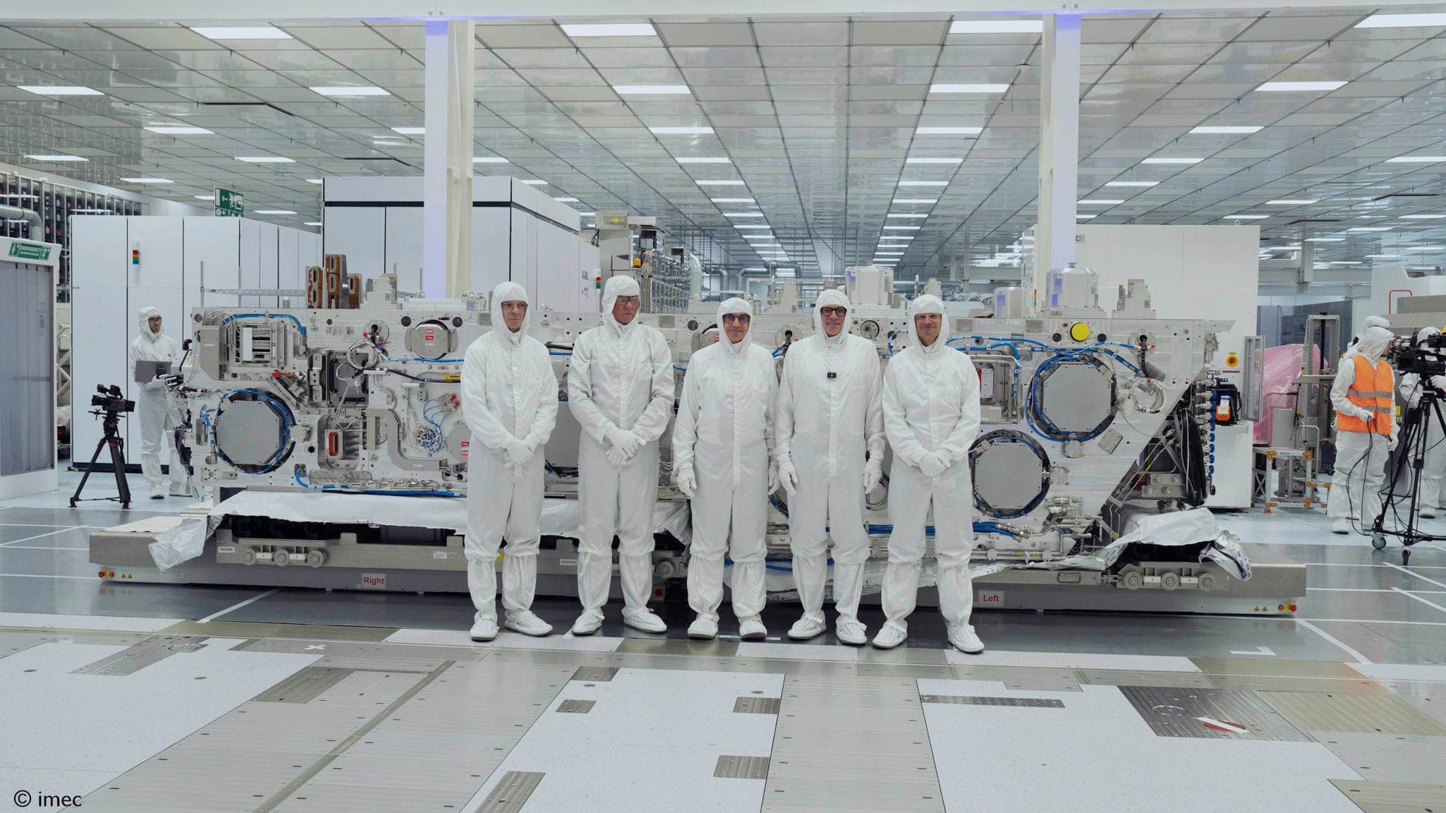
Imec receives the world’s most advanced High NA EUV system
A major milestone in propelling industry into the ångström era
Read more
ITF USA 2026 at SEMICON® West
From silicon to systems: building the AI future The pace of AI evolution leaves little room for certainty. Yet, several trends are clear: AI agents increasingly collaborating in orchestrated ecosystems are on the rise. Physical AI is a crucial next step, including (humanoid) robots transforming our homes and workspaces. In parallel, AI – just like advances in quantum computing – could help unlock breakthroughs in fields such as physics and biology. Building the AI future starts with a solid hardware foundation – from high-performance, energy-efficient compute in the data centers to low-power, real-time inference at the edge. ITF USA at SEMICON® West presents the building blocks for shaping the AI future. On October 12 in San Francisco, we take stock of the full AI deep-tech stack: from silicon to systems, from research to manufacturing. Discover ITF USA
View event