Imec unlocks lever for EUV dose reduction: oxygen injection during metal-oxide resist post-exposure bake emerges as game-changer for throughput
The findings reveal that controlling gas composition, especially oxygen levels, during critical lithography steps dramatically optimizes metal-oxide resist performance for next-generation, high-throughput EUV patterning.
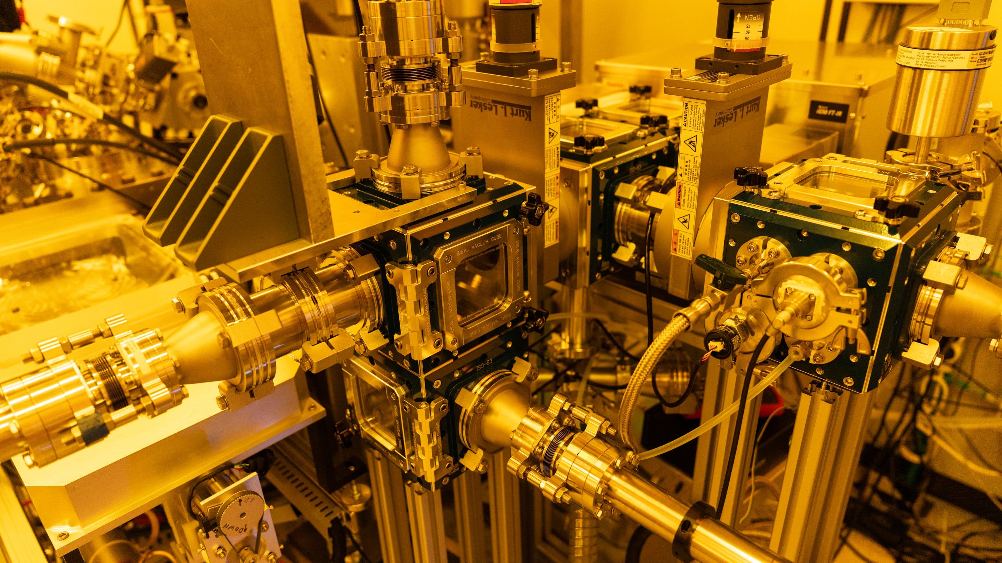
LEUVEN (Belgium), FEBRUARY 25, 2026—This week, at the 2026 SPIE Advanced Lithography + Patterning Conference, imec, a world-leading research and innovation hub in advanced semiconductor technologies, demonstrates that precise control of gas compositions during post-exposure EUV lithography steps can help in minimizing the required exposure dose, thereby unlocking higher wafer throughput. In particular, improved dose response of metal-oxide photoresists (MORs) has been achieved when the EUV post-exposure bake step is performed under elevated oxygen concentrations.
Metal-oxide resists (MORs) have emerged as leading candidates for advanced EUV lithography applications, offering superior resolution, reduced line-edge roughness, and good EUV dose-to-size performance compared to chemically amplified resists (CARs). Their better pattern transfer capability for small features and thin resist films makes them particularly attractive for the highest resolution metal layers, exposed using High NA EUV lithography.
Imec now demonstrates that the dose response of MORs can be further improved by raising the oxygen concentration above atmospheric levels during the EUV lithography post-exposure bake step – a critical heat treatment step after EUV resist exposure and before resist development.
Ivan Pollentier, senior researcher at imec: “We observe a 15-20% faster photo-speed when increasing the oxygen concentration from atmospheric 21% to 50% during post-exposure bake. The trend is observed for both model MOR and commercial MOR materials. This finding shows for the first time that carefully controlling the gas composition during key lithography steps can significantly cut the required EUV exposure dose, directly boosting the throughput of the EUV scanner and reducing process costs. This is just a first result from the BEFORCE tool: the controlled gas composition provides an additional knob to study the origins of environmental effects on the lithographic variability of MOR materials. Equipment manufacturers can use these insights as a guideline to adapt their tools for improved EUV lithography throughput and stability.”
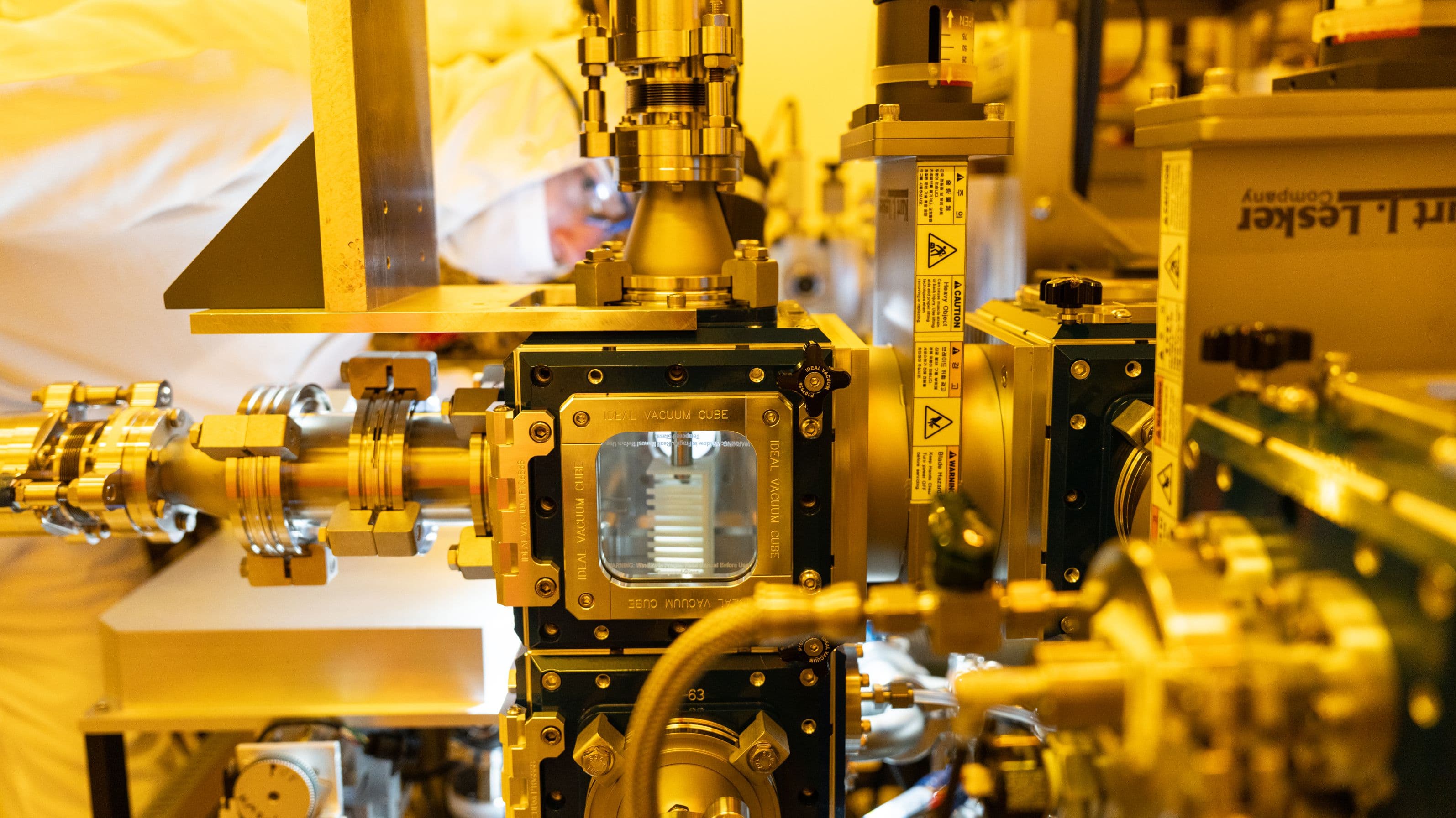
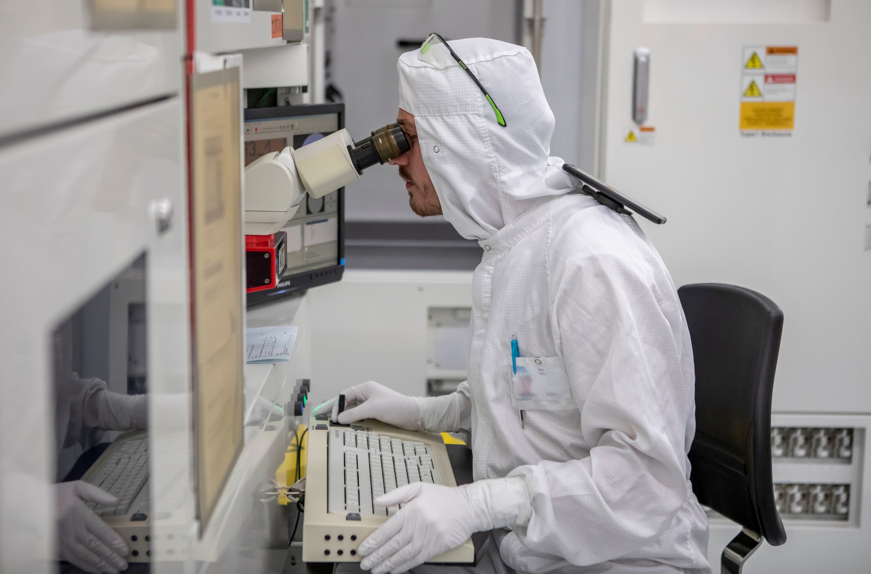
The results were achieved using BEFORCE, a unique research tool developed by imec to investigate the role of the ambient environment on critical dimension (CD) stability and performance of MORs. Kevin Dorney, R&D team lead at imec: “In commercial EUV clusters, resist-coated wafers are exposed in vacuum and then transferred to the post-exposure bake unit, where they are heated under atmospheric conditions. Our BEFORCE tool mimics these operations, but the wafer transfer and post-exposure bake are isolated from the cleanroom atmosphere and can be performed in precisely controlled environments allowed by gas injection and mixing systems. This unique ability, in combination with an integrated photo-speed measurement, was key to revealing the role of oxygen in boosting MOR’s dose response.”
To optimally exploit the positive impact of gas compositions on the MOR performance, a more fundamental understanding of the chemical mechanism at play during the resist’s post-exposure bake is essential. Experiments are ongoing to correlate MOR performance to observations of chemical changes during bake – captured by an integrated Fourier transform infrared spectrometer – under varying environmental conditions. The planned expansion of the BEFORCE tool with advanced metrology capabilities will enable imec to drive even more impactful results.
BEFORCE can be used more broadly to study both MOR and CAR resists and is accessible to imec’s partners for resist evaluation.
The presented achievements and preliminary fundamental insights are shared in two papers at the 2026 SPIE Advanced Lithography + Patterning Conference:
This work has been enabled in part by the NanoIC pilot line. The acquisition and operation are jointly funded by the Chips Joint Undertaking, through the European Union’s Digital Europe (101183266) and Horizon Europe programs (101183277), as well as by the participating states Belgium (Flanders), France, Germany, Finland, Ireland and Romania. For more information, visit nanoic-project.eu.
About imec
Imec is a world-leading research and innovation hub in advanced semiconductor technologies. Leveraging its state-of-the-art R&D infrastructure and the expertise of over 6,500 employees, imec drives innovation in semiconductor and system scaling, artificial intelligence, silicon photonics, connectivity, and sensing.
Imec’s advanced research powers breakthroughs across a wide range of industries, including computing, health, automotive, energy, infotainment, industry, agrifood, and security. Through IC-Link, imec guides companies through every step of the chip journey - from initial concept to full-scale manufacturing - delivering customized solutions tailored to meet the most advanced design and production needs.
Imec collaborates with global leaders across the semiconductor value chain, as well as with technology companies, start-ups, academia, and research institutions in Flanders and worldwide. Headquartered in Leuven, Belgium, imec has research facilities across Belgium and in Germany, the Netherlands, Italy, the UK, Spain, and the USA, with representation on three continents. In 2024, imec reported revenues of €1.034 billion.
For more information, visit www.imec-int.com
The imec group holds a global trademark portfolio, including word marks and combined figurative registered and unregistered trademarks, across national, regional, and international territories. Its lawful use requires prior written consent of IMEC in compliance with the IMEC branding guidelines, which may be updated periodically. The latest version is available upon written request.
Discover more

Imec achieves new milestones in single patterning High NA EUV lithography for both damascene and direct metal etch metallization processes
Read more
Imec and ZEISS intensify collaboration with the signing of a new Strategic Partnership Agreement
Read more