Imec and ZEISS intensify collaboration with the signing of a new Strategic Partnership Agreement
- The signed Strategic Partnership Agreement extends the existing strategic partnership between imec and ZEISS, which has been in place since 2019, until 2029.
- With the investments in imec's pilot line, ZEISS significantly contributes to the research and further development of key semiconductor technologies and the technological innovation advantage of Europe, aligning with the goals and ambitions of the European Union and the European Chips Act.
- The strong cohesion among European partners, like imec and ZEISS, is crucial in setting up the NanoIC pilot line, the most advanced infrastructure for sub-2nm research and development in the world
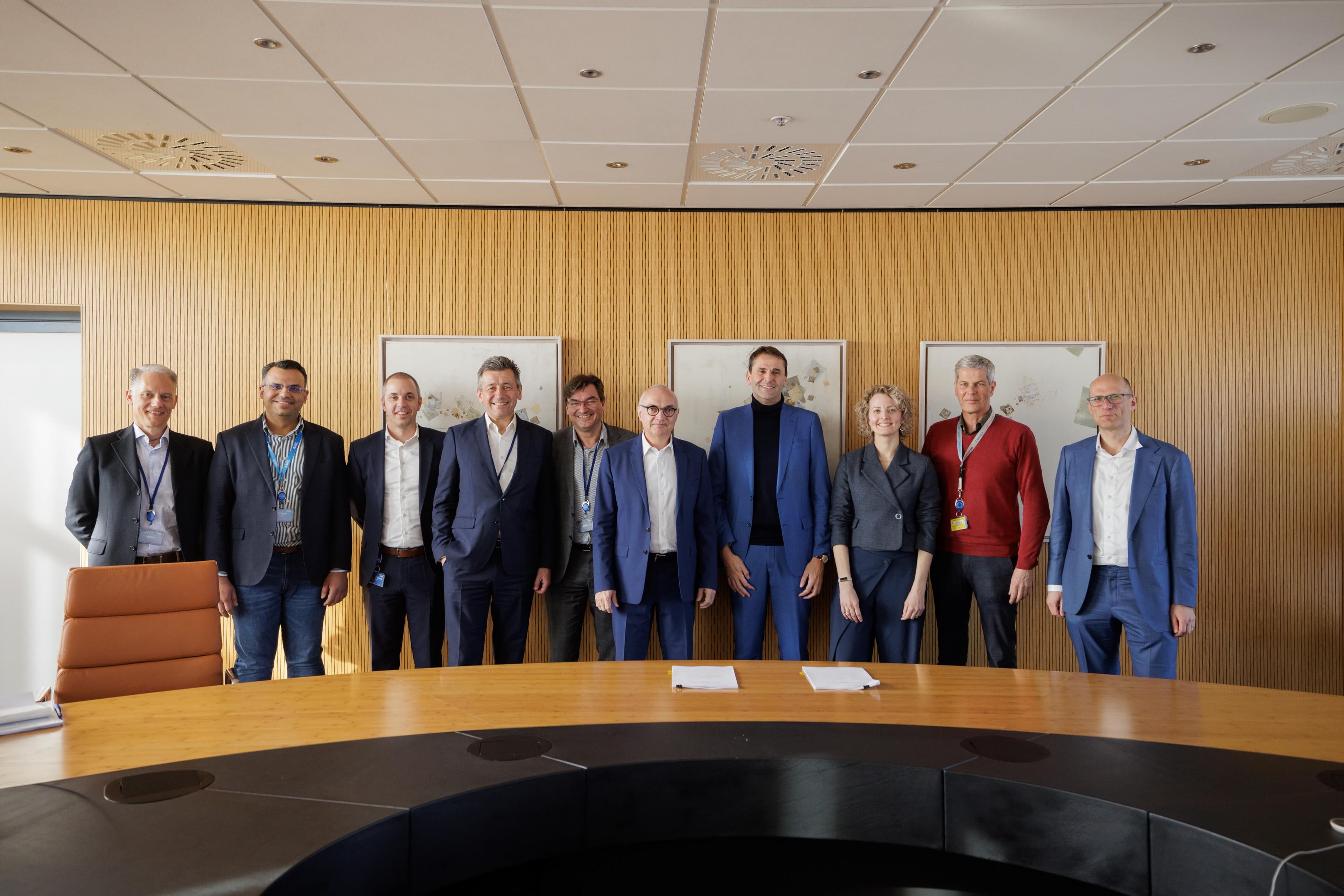
Leuven (Belgium) and Oberkochen (Germany), March 20, 2025 - Imec, a world-leading research and innovation hub in nanoelectronics and digital technologies, and ZEISS Semiconductor Manufacturing Technology (SMT), a leading technology company in the optical and optoelectronic industry and supplier of key components for the production of microchips, are intensifying their collaboration to advance the NanoIC pilot line at imec with state-of-the-art semiconductor technology and manufacturing expertise for sub-2nm research and development. Therefore, both parties have signed a Strategic Partnership Agreement (SPA).
Strong cooperation for tomorrow's semiconductor manufacturing technologies
The signed Strategic Partnership Agreement extends the existing strategic partnership between imec and ZEISS, which has been in place since 2019, until 2029. "We are very pleased to intensify our collaboration with imec to jointly advance the semiconductor technologies of tomorrow with its strong partner network," explains Thomas Stammler, Chief Technology Officer and member of the Management Team of ZEISS SMT. Since 1997, imec and the ZEISS segment Semiconductor Manufacturing Technology have been working on various joint projects to further develop Moore's Law, which continues to drive the ongoing increase in the performance of microchips and memory processors. "For the research and development of cutting-edge semiconductor technologies, the expertise and technological experience of industry partners like ZEISS is essential. Therefore, we are very pleased to strengthen our partnership even further," says Luc Van den hove, President and Chief Executive Officer of imec.
With the signed agreement, the two cooperation partners reaffirm their joint efforts to advance key semiconductor manufacturing technologies such as High-NA EUV lithography. This technology will enable the production of even more powerful and energy-efficient microchips, which are the foundation for key technologies such as artificial intelligence, autonomous driving, Industry 4.0, and groundbreaking solutions for medical technology and the energy transition.
Imec's pilot line as a research center for the global semiconductor industry
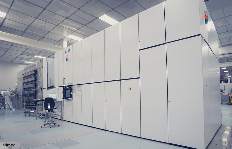
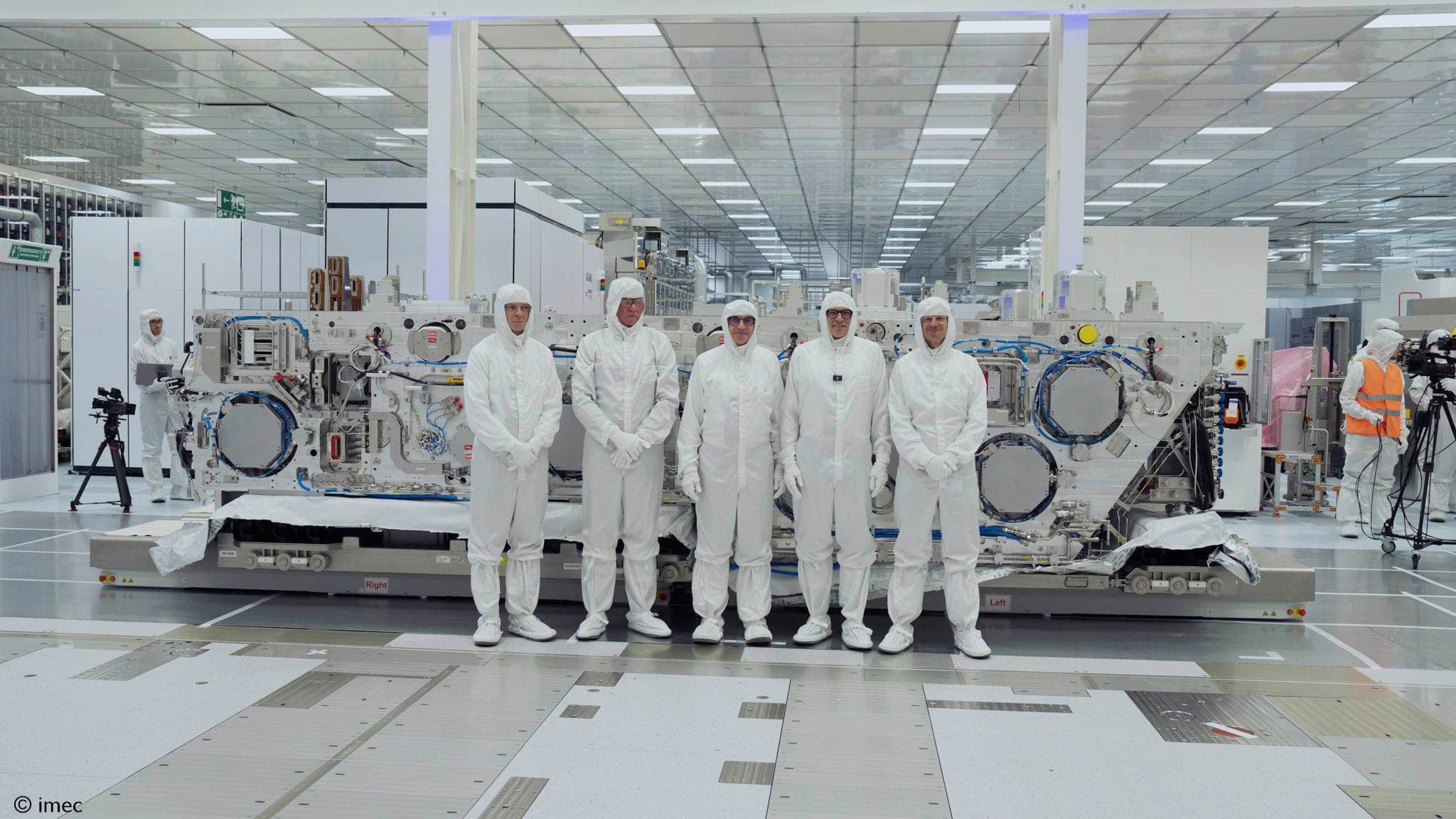
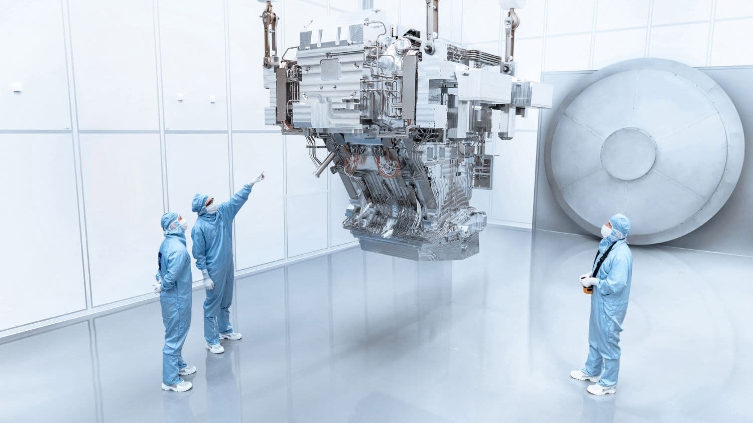
As part of the agreement, ZEISS supports imec not only by participating in research projects to advance manufacturing, process, and measurement technologies for semiconductor manufacturing but also by providing lithography optics, integrated into the lithography scanner systems of the strategic partner ASML, of various product generations for imec's pilot line, which is an essential part of the cooperation.
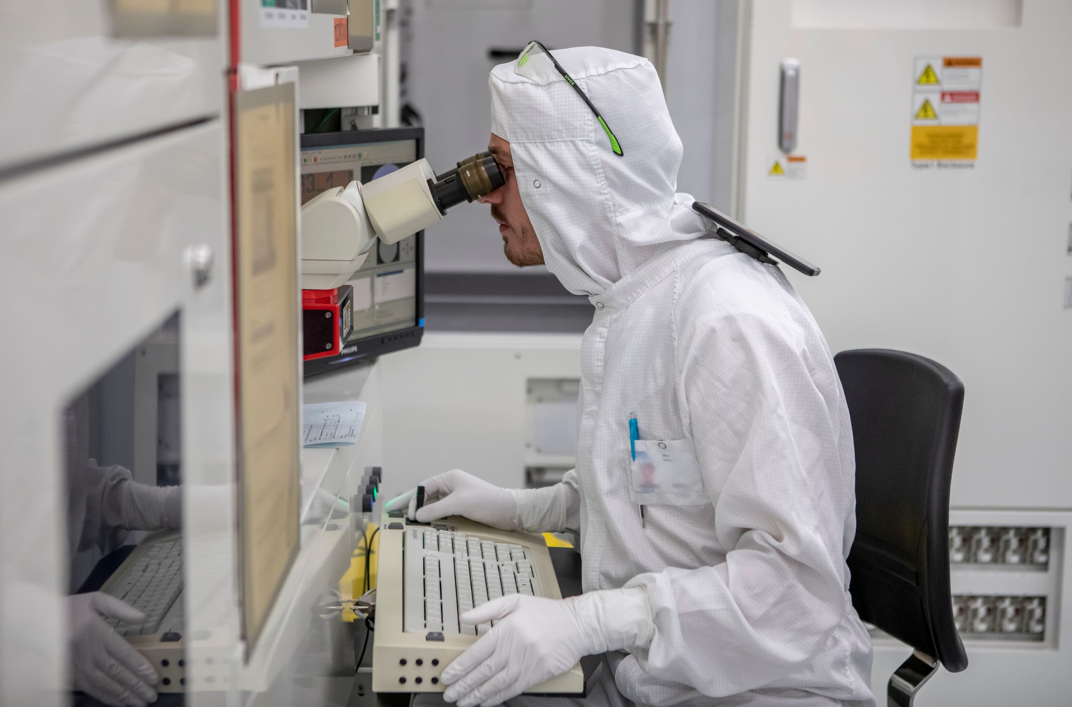
Imec's pilot line, now being expanded with the NanoIC pilot line, operated in Leuven, Belgium, encompasses the entire value creation process as well as various technology strands for semiconductor manufacturing. It aims to provide industry representatives such as end customers, suppliers, and research institutions access to pioneering and advanced semiconductor technologies and platforms, enabling them to explore, develop, and test innovations. The optimization of existing equipment, processes, and measurement methods is also being advanced to enable ever smaller, more powerful, and energy-efficient microchips, thereby driving global digitalization. The collaboration is deepened through ZEISS's involvement in various industry partner programs, such as advanced patterning, 3D system integration, and optical interconnect, under the leadership of imec. In these programs, work is being done together on the latest process and inspection methods for process optimizations of next-generation semiconductors.
Investments in line with the European Chips Act
The close collaboration between imec and ZEISS aligns with the goals and ambitions of the European Union and the European Chips Act, which aims to strengthen Europe's technological sovereignty, competitiveness, and resilience. "With the investments in imec's pilot line, now being expanded with the NanoIC pilot line, ZEISS is significantly contributing to maintaining Europe's lead in the latest generation of semiconductor equipment and further expanding it through the development of technology roadmaps," says Stammler.
The strengthened cooperation between the two partners also sends a signal regarding the relevance of cross-industry networking for the global semiconductor market: “This strategic partnership between imec and ZEISS underscores how strong cohesion among European partners, which is crucial in setting up the NanoIC pilot line, the most advanced infrastructure for sub-2nm research and development in the world, accelerates innovation and strengthens Europe’s leadership position in the semiconductor ecosystem," says Van den hove.
The acquisition and operation of the NanoIC pilot line are jointly funded by the Chips Joint Undertaking, through the European Union’s Digital Europe (101183266) and Horizon Europe programs (101183277), as well as by the participating states Belgium (Flanders), France, Germany, Finland, Ireland and Romania. For more information, visit www.nanoic-project.eu.


About ZEISS
ZEISS is an internationally leading technology enterprise operating in the fields of optics and optoelectronics. In the previous fiscal year, the ZEISS Group generated annual revenue around 11 billion euros in its four segments Semiconductor Manufacturing Technology, Industrial Quality & Research, Medical Technology and Consumer Markets (30 September 2024).
For its customers, ZEISS develops, produces and distributes highly innovative solutions for industrial metrology and quality assurance, microscopy solutions for the life sciences and materials research, and medical technology solutions for diagnostics and treatment in ophthalmology and microsurgery. The name ZEISS is also synonymous with the world's leading lithography optics, which are used by the chip industry to manufacture semiconductor components. There is global demand for trendsetting ZEISS brand products such as eyeglass lenses, camera lenses and binoculars.
With a portfolio aligned with future growth areas like digitalization, healthcare and Smart Production and a strong brand, ZEISS is shaping the future of technology and constantly advancing the world of optics and related fields with its solutions. The company's significant, sustainable investments in research and development lay the foundation for the success and continued expansion of ZEISS' technology and market leadership. ZEISS invests 15 percent of its revenue in research and development – this high level of expenditure has a long tradition at ZEISS and is also an investment in the future.
With over 46,000 employees, ZEISS is active globally in around 50 countries with more than 60 sales and service locations, around 40 research and development facilities, and 35 production facilities worldwide (30 September 2024). Founded in 1846 in Jena, the company is headquartered in Oberkochen, Germany. The Carl Zeiss Foundation, one of the largest foundations in Germany committed to the promotion of science, is the sole owner of the holding company, Carl Zeiss AG.
Further information at www.zeiss.com
ZEISS Semiconductor Manufacturing Technology
With its product portfolio and expertise, the Semiconductor Manufacturing Technology segment of ZEISS covers a variety of key processes in the production of microchips. Its products include semiconductor manufacturing optics – notably lithography optics – as well as photomask systems and process control solutions for semiconductor manufacturing. Thanks to ZEISS technology, microchips are becoming increasingly smaller, more powerful, more energy-efficient and more affordable. The electronic applications of these ongoing enhancements enable global progress in many disciplines such as technology, electronics, communication, entertainment, mobility and energy. Semiconductor Manufacturing Technology is headquartered in Oberkochen. Other sites include Jena, Rossdorf, Wetzlar, Aachen and Coswig (Germany), Zurich (Switzerland), as well as Bar Lev (Israel) and Dublin, CA (USA).
About imec
Imec is a world-leading research and innovation center in nanoelectronics and digital technologies. Imec leverages its state-of-the-art R&D infrastructure and its team of more than 6,000 employees and top researchers, for R&D in advanced semiconductor and system scaling, silicon photonics, artificial intelligence, beyond 5G communications and sensing technologies, and in application domains such as health and life sciences, mobility, industry 4.0, agrofood, smart cities, sustainable energy, education, … Imec unites world-industry leaders across the semiconductor value chain, Flanders-based and international tech, pharma, medical and ICT companies, start-ups, and academia and knowledge centers. imec is headquartered in Leuven (Belgium), and has research sites across Belgium, in the Netherlands, and representation in 3 continents. In 2023, imec's revenue (P&L) totaled 941 million euro.
Further information at www.imec-int.com
The imec group holds a global trademark portfolio, including word marks and combined figurative registered and unregistered trademarks, across national, regional, and international territories. Its lawful use requires prior written consent of IMEC in compliance with the IMEC branding guidelines, which may be updated periodically. The latest version is available upon written request.