Imec launches university consortium around next generation of chips
Leveraging European academic excellence to accelerate industrial innovation.

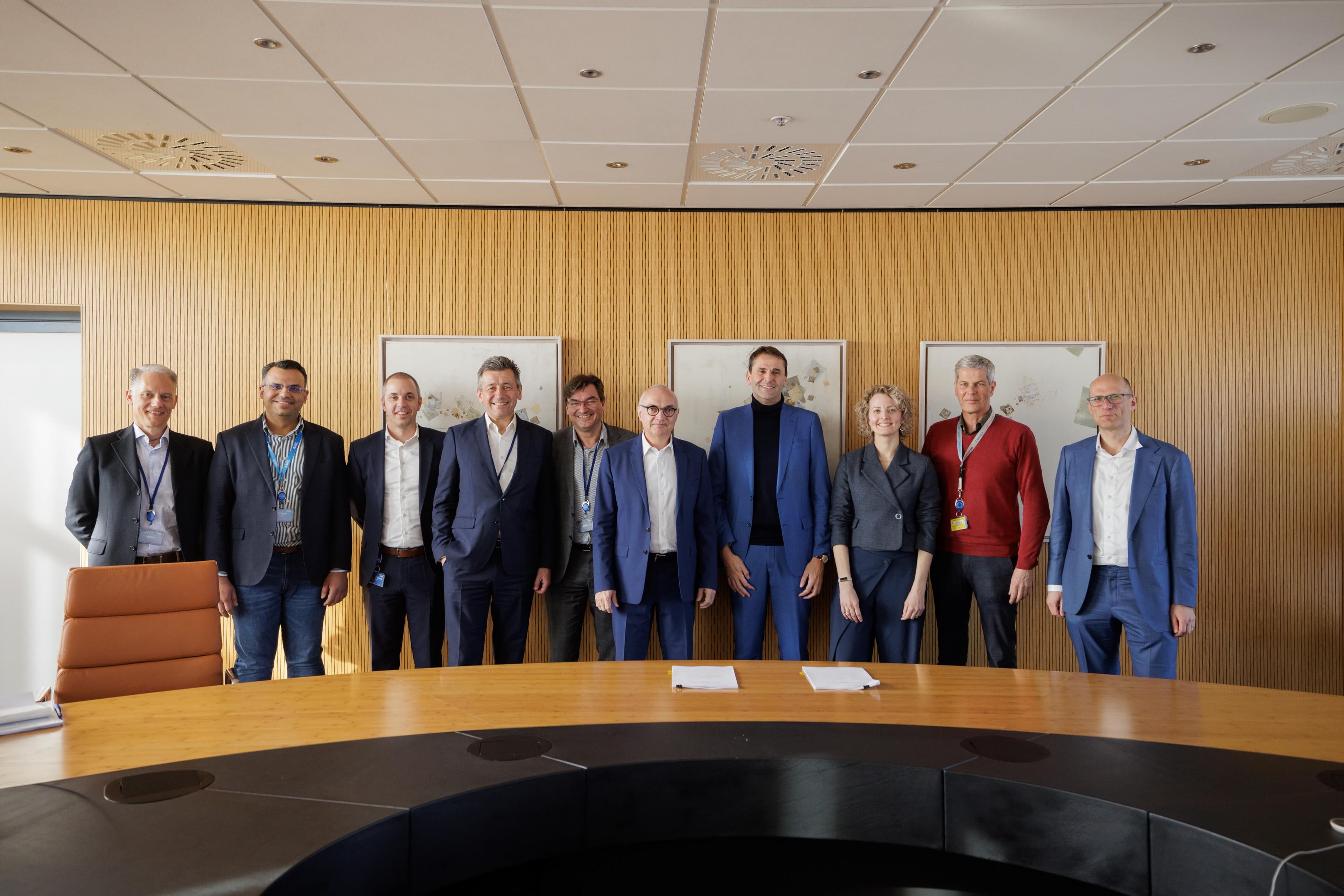
LEUVEN (Belgium), MARCH 12th, 2026— Imec, a world-leading research and innovation hub in advanced semiconductor technologies, has launched a first-of-its-kind consortium with 26 European university groups that will jointly work on the technology roadmap beyond CMOS scaling (CMOS 2.0). This initiative will focus on design automation and chip architecture research for the next generation of chips. The consortium will benefit from the NanoIC pilot line, turning academic insights into industry-focused innovations. In the future, similar consortia will be set up around advanced materials and alternative compute systems.
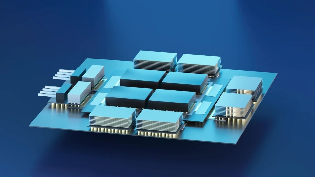
CMOS 2.0 refers to a new paradigm, introduced by imec, that expands the chipmaking toolbox beyond traditional transistor scaling and its associated scaling challenges. CMOS 2.0 allows for more design flexibility by exploiting fine-grain wafer stacking technology to improve on-chip connectivity and offer higher technology heterogeneity to the system. It will result in tailored chips comprising multiple 3D-stacked layers that fulfil smartly partitioned functions. In that way, CMOS 2.0 will provide advanced, versatile 3D stacked platforms that push the boundaries of compute performance.
Introducing this new paradigm will have profound implications on how computing architectures are designed and optimized for future workloads and applications. CMOS 2.0 is a key differentiator for the realization of next-generation energy-efficient compute systems and is expected to impact a wide variety of applications from general-purpose processors to high-performance AI computing systems and even further for embedded AI applications at the edge.
This strategically important research requires cross-pollination between different areas of the ecosystem. Within imec’s CMOS 2.0-consortium, 26 PhDs will be funded. The PhD students will stay at their home university, embedded in their research groups, allowing them to tap into complementary fields of expertise and stimulate cross-fertilization. The participating universities and imec will jointly develop the necessary know-how that lays down the foundation of the next-generation CMOS technology platforms and their associated compute architectures. Moreover, the collaboration will support workforce and skill development in Europe to meet current and future industry needs.
Sahar Sahhaf, director academic partnership development:“The attraction for the concept of CMOS 2.0 is clear, but the obstacles are equally substantial. Leveraging the benefits in both connectivity and heterogeneous integration enabled by 3D wafer stacking will reshape every stage of design and chip architecture. It requires convergence of expertise, close collaboration, and coordination. It's the first time that imec brings together such a network of premium European university teams in a structured way to have guided contributions to the future semiconductor roadmap. We are excited to further connect academic inputs in our industry-driven programs to put Europe in the forefront of research on advanced computing technologies.”
Mehdi Tahoori, technical director:"This university research consortium aims to infuse CMOS 2.0 technology to the entire design stack, from electronic design automation (EDA) all the way to system architecture. It aims to stimulate the broader research and academic community on various aspects of the CMOS 2.0 revolution. Imec plays a unique and crucial role by linking academic research to industry needs, and by extending the roadmap of technology scaling with CMOS 2.0.”
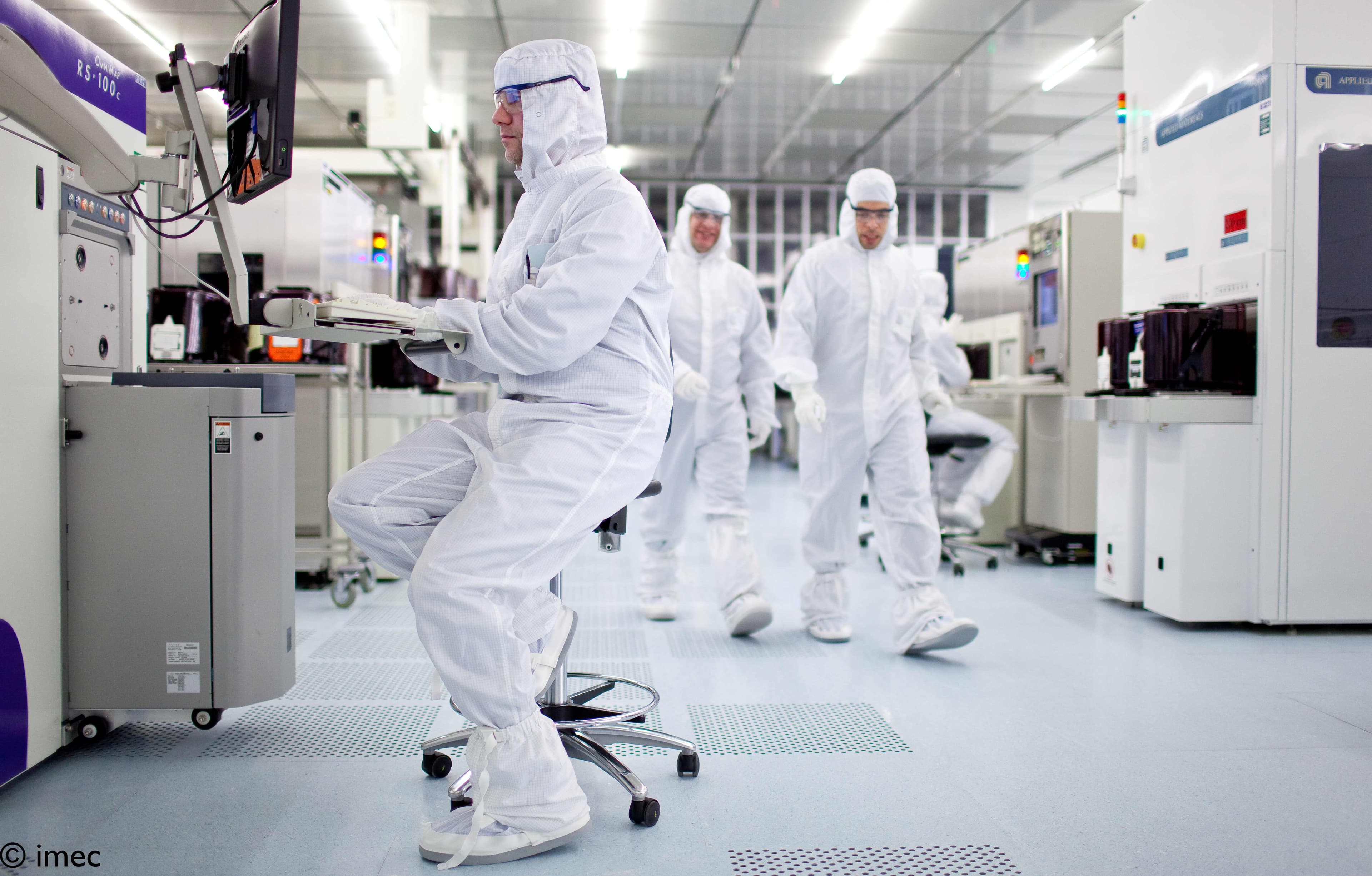
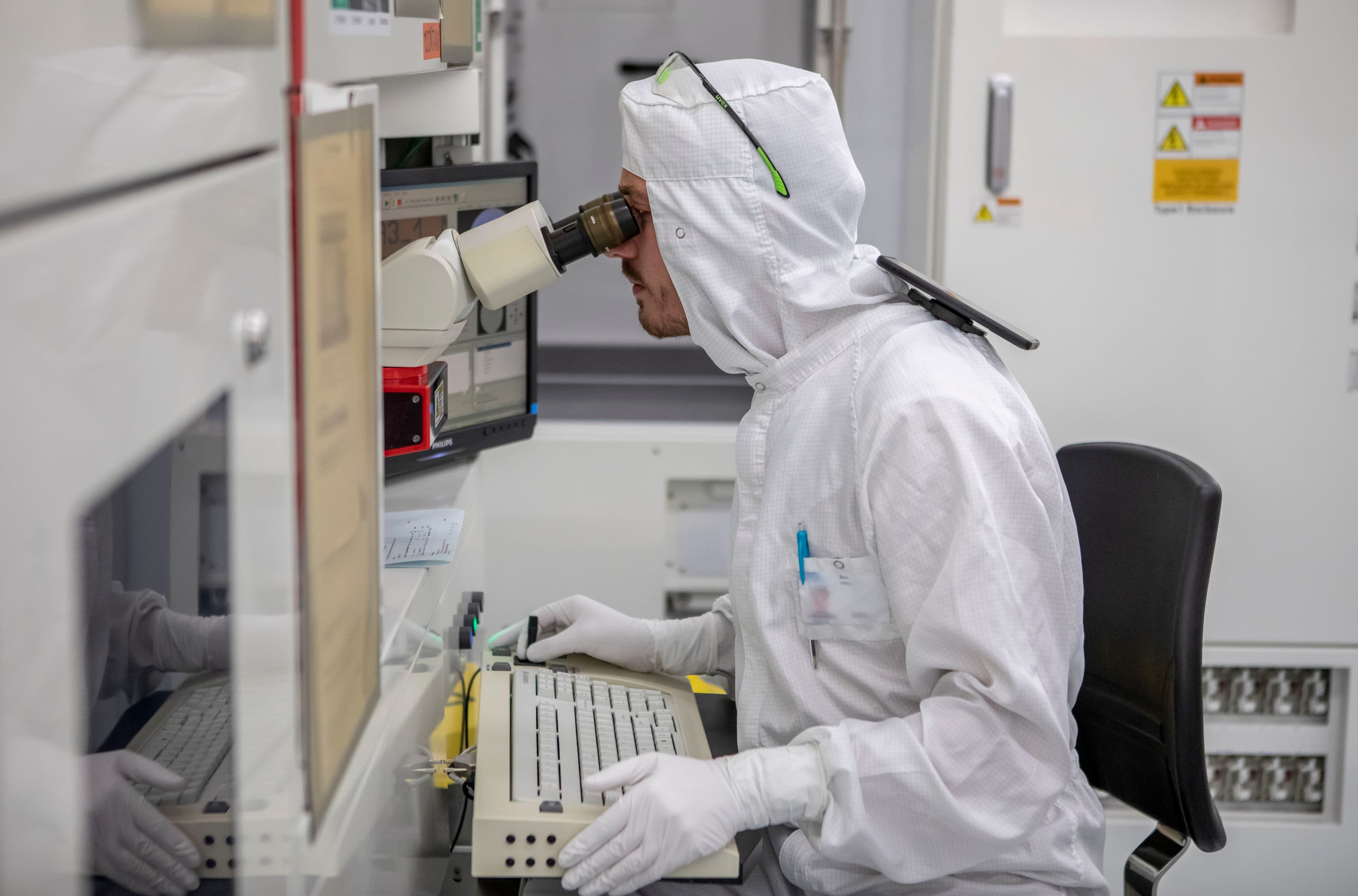
Of particular importance is the presence of the NanoIC pilot line hosted by imec in Leuven and its decisive role in empowering the CMOS 2.0 academic consortium. Its state‑of‑the‑art tools are embedded within a strong, collaborative ecosystem of industry partners. PhD students can gain early exposure to next-generation semiconductor logic, memory and 3D technologies through process design kits (PDKs), which will enable them to develop system‑level thinking; which is typically only encountered much later in a research or industrial career.
As such, it bridges the gap from academia to industry, facilitating a rapid transfer of knowledge and advanced technology from research labs to the market, thus strengthening Europe’s industry.
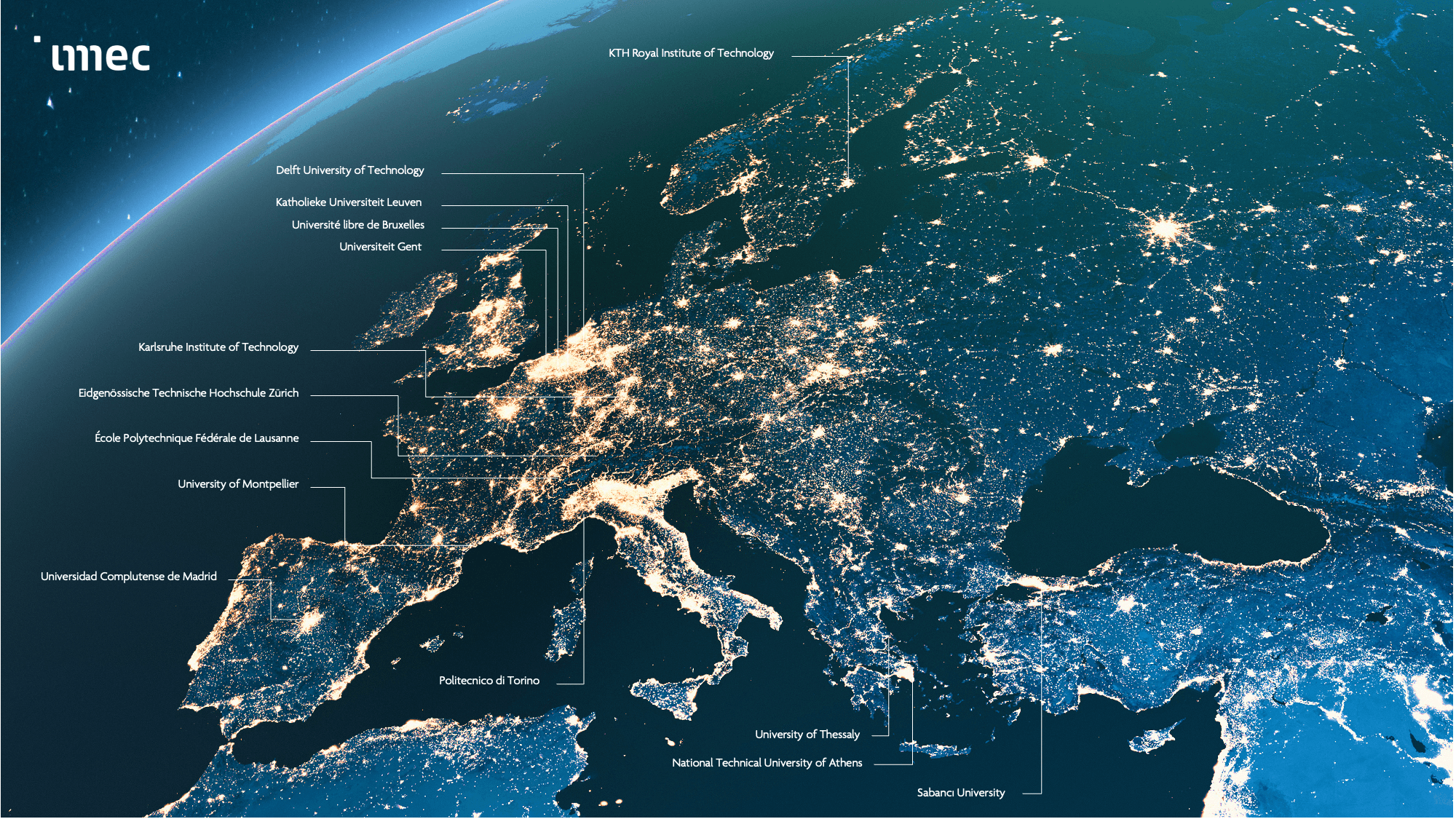
The CMOS 2.0 university consortium consists of following universities:
National Technical University of Athens
Delft University of Technology
École Polytechnique Fédérale de Lausanne (EPFL)
Eidgenössische Technische Hochschule Zürich
Karlsruhe Institute of Technology
Katholieke Universiteit Leuven
KTH Royal Institute of Technology
LIRMM, University of Montpellier, CNRS
Politecnico di Torino
Sabancı University
Universidad Complutense de Madrid
Universiteit Gent
Université libre de Bruxelles
University of Thessaly
About imec
Imec is a world-leading research and innovation hub in advanced semiconductor technologies. Leveraging its state-of-the-art R&D infrastructure and the expertise of over 6,500 employees, imec drives innovation in semiconductor and system scaling, artificial intelligence, silicon photonics, connectivity, and sensing.
Imec’s advanced research powers breakthroughs across a wide range of industries, including computing, health, automotive, industry, consumer electronics, aerospace and security. Through IC-Link, imec guides companies through every step of the chip journey - from initial concept to full-scale manufacturing - delivering customized solutions tailored to meet the most advanced design and production needs.
Imec collaborates with global leaders across the semiconductor value chain, as well as with technology companies, start-ups, academia, and research institutions in Flanders and worldwide. Headquartered in Leuven, Belgium, imec has research facilities in Belgium, across Europe, the USA and the GCC region, and representation on three continents. In 2024, imec reported revenues of €1.034 billion.
The imec group holds a global trademark portfolio, including word marks and combined figurative registered and unregistered trademarks, across national, regional, and international territories. Its lawful use requires prior written consent of IMEC in compliance with the IMEC branding guidelines, which may be updated periodically. The latest version is available upon written request.