NanoIC adds advanced SRAM memory macros to its N2 pathfinding PDK
Major update of NanoIC’s Pathfinding N2 P-PDK empowers researchers and designers to learn and innovate on full SoC architectures

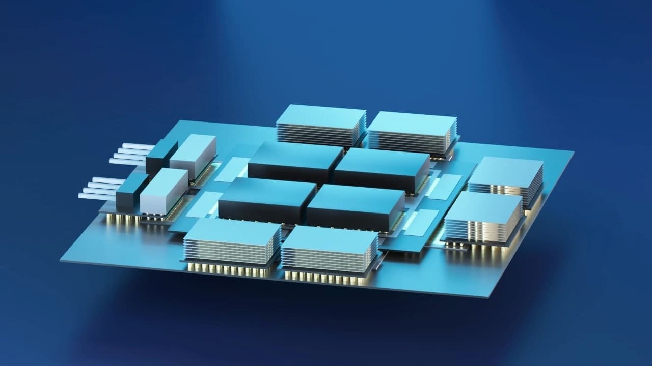
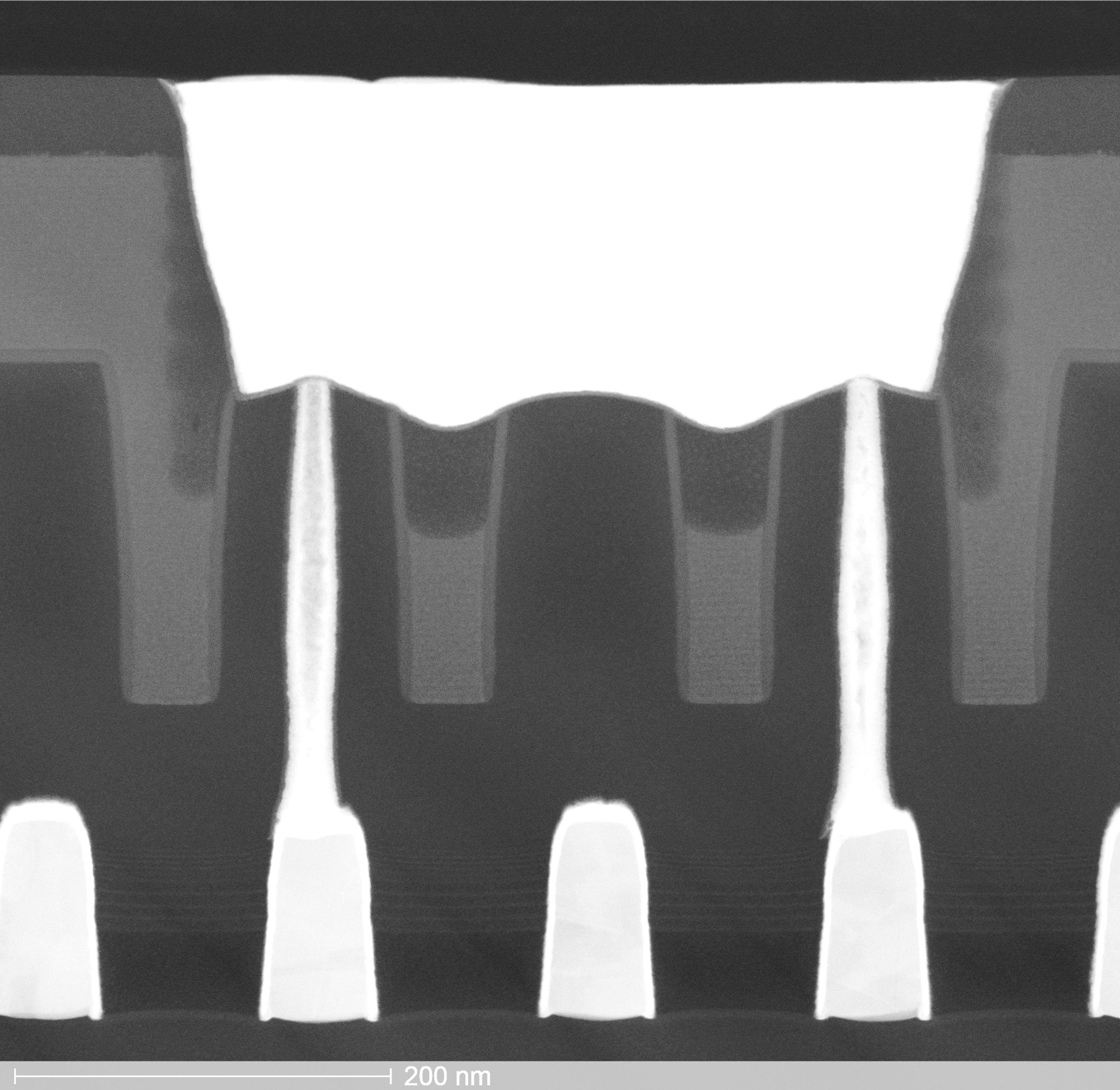
LEUVEN (Belgium), NOVEMBER 18, 2025 — This week, at SEMICON Europa, the NanoIC pilot line, a European initiative coordinated by imec and dedicated to accelerating innovation in chip technologies beyond 2nm, announces the release of the N2 P-PDK v1.0, an important update of its N2 Pathfinding Process Design Kit (P-PDK). This new version introduces several new features, including a library of 29 SRAM memory macros, allowing designers to explore and benchmark system-on-chip (SoC) designs with frontside and backside power routing. By adding the SRAM macros in the design options, the N2 P-PDK v1.0 marks an important milestone in enabling research, learning, and design exploration on advanced and future nodes.
Towards next-generation SoC designs
As chip technologies scale beyond 2nm, the ability to explore full system-on-chip (SoC) architectures with novel technology enablers becomes increasingly important.
SoCs, integrating logic, memory, and interconnect capabilities into a single chip, are the backbone of a wide variety of digital applications, from smartphones and AI accelerators to automotive controllers. However, early-stage SoC design exploration is often constrained by limited access to complete and realistic design kits that include advanced or future technology scaling boosters such as power delivery networks.
This gap makes it difficult for designers to validate architectural concepts, experiment with emerging technologies, or to train the next generation of chip designers on advanced nodes.
NanoIC’s low-barrier N2 P-PDK v1.0 aims to bridge this gap, offering instant access to a wide variety of new design features, including a portfolio of 29 ready-to-use SRAMmacros with both frontside and backside power routing configurations.
This dual configuration, offered for the first time in a pathfinding PDK, enables designers to experiment with and optimize memory integration within realistic, advanced power networks. As a result, NanoIC’s N2 P-PDK v1.0 now provides the building blocks of a complete SoC as well as the architectural context to explore how those blocks interact within realistic power networks.
It enables users to move beyond simple logic design and explore and validate full SoC systems that reflect the challenges and opportunities of next-generation semiconductor design.
Lowering barriers for learning and exploration
By making these advanced features freely available to academic researchers, startups, and design teams, NanoIC significantly lowers the barriers to innovation, empowering the development of next-generation applications, and strengthening Europe’s position in the global semiconductor landscape.
“This v1.0 version of our N2 P-PDK enables designers to evaluate the impact of new technology features and integration options on their designs before they exist in foundry offerings. It provides a unique environment to connect technology pathfinding with practical design enablement, ensuring that breakthroughs in device research translate into system-level advances.”,Marie Garcia Bardon, department director at imec and work package leader within the NanoIC pilot line, summarizes.
Building on the learnings from the previous N2 P-PDK, this release lays the groundwork for future PDK iterations, launching additional advanced logic, memory, and interconnect PDKs in the coming years.
The roadmap includes future versions of the N2 P-PDK, as well as upcoming A14 and A7 logic P-PDKs, eDRAM and SOT memory PDKs, and advanced interconnect solutions (RDL, hybrid bonding, interposers), empowering innovation across the full spectrum of next-generation chip technologies.
To support designers in exploring the full capabilities of the N2 P-PDK v1.0, a dedicated workshop will be organized on March 25-26, 2026. This session will offer a theoretical framework, followed by hands-on training sessions, using two different EDA tools: Cadence and Synopsys.
Participants will gain insights into the SRAM memory macros, updated design rules, and system-level integration strategies. More details and registration will be made available via the NanoIC website.
About the NanoIC pilot line
The NanoIC pilot line is a pioneering European initiative, hosted by imec, set to provide a leading-edge beyond 2nm System-on-Chip (SoC) pilot line for advanced logic, memory, and interconnect technologies. The project aims to drive European technology leadership across critical markets such as computing, communication, mobility, energy, and health. The pilot line is a collaboration between imec, CEA-Leti, Fraunhofer-Gesellschaft, VTT, CSSNT-UPB, and Tyndall Institute and is supported by the Chips Joint Undertaking, through the European Union’s Digital Europe (101183266) and Horizon Europe programs (101183277), as well as by the participating states Belgium (Flanders), France, Germany, Finland, Ireland and Romania. For more details, please visit nanoic-project.eu.
About imec
Imec is a world-leading research and innovation hub in advanced semiconductor technologies. Leveraging its state-of-the-art R&D infrastructure and the expertise of over 6,000 employees, imec drives innovation in semiconductor and system scaling, artificial intelligence, silicon photonics, connectivity, and sensing.
Imec’s advanced research powers breakthroughs across a wide range of industries, including computing, health, automotive, energy, infotainment, industry, agrifood, and security. Through IC-Link, imec guides companies through every step of the chip journey - from initial concept to full-scale manufacturing - delivering customized solutions tailored to meet the most advanced design and production needs.
Imec collaborates with global leaders across the semiconductor value chain, as well as with technology companies, start-ups, academia, and research institutions in Flanders and worldwide. Headquartered in Leuven, Belgium, imec has research facilities across Belgium and in Germany, the Netherlands, Italy, the UK, Spain, and the USA, with representation on three continents. In 2024, imec reported revenues of €1.034 billion.
For more information, visitwww.imec-int.com
The imec group holds a global trademark portfolio, including word marks and combined figurative registered and unregistered trademarks, across national, regional, and international territories. Its lawful use requires prior written consent of IMEC in compliance with the IMEC branding guidelines, which may be updated periodically. The latest version is available upon written request.