Tackling the talent shortage for European deep tech: a matter of alignment, outreach, ... and persistence
Talent shortages are fast becoming a critical barrier to Europe’s semiconductor ambitions. Annelies Daenen, Director of Talent Development at imec, explores the scale of the challenge and the steps needed to close the gap.

This article appeared earlier in the European.
The figures from the latest Skills Strategy report by the European Chips Skills Academy (ECSA) speak volumes. Talent shortages are becoming a major bottleneck to further develop this highly strategic part of Europe’s future industry. How big is the problem? And more importantly, what can be done about it?
271,400 European job vacancies by 2030
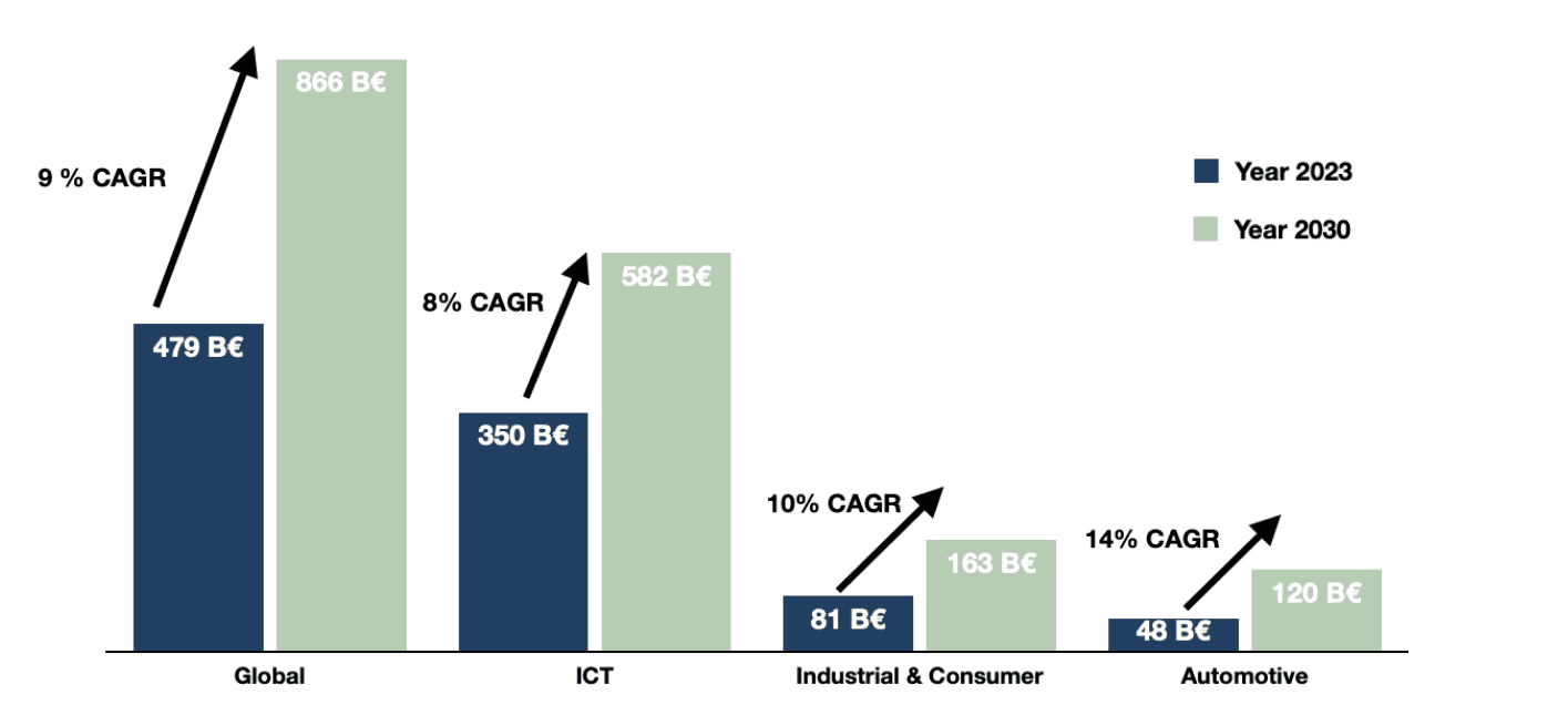
The expected growth in European production, driven by AI and digitalization, is expected to lead to a significant increase in jobs in the semiconductor industry by 2030. The growth of the sector is driven by the industry itself, as well as by European policy. The EU Chips Act considers the semiconductor sector a key driver of the future economy and a crucial component in preserving our core industries in a global market.
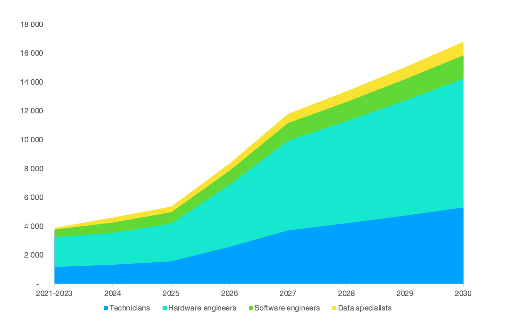
The European Chips Skills Academy (ECSA) report predicts that an additional 155,900 jobs will be created between now and 2030, despite a significant trend toward automation in the sector. Due to the expected outflow of workers through retirement and demographic trends, this figure climbs to 271,400 job openings, primarily for technical roles. Even today, it is challenging to fill vacancies, and the talent gap is likely to widen further in the years to come.
Boosting the industry-readiness of academia
Part of the explanation for this talent gap is a mismatch between academia and industry in terms of skill sets. An academic environment differs significantly from that of a fab, which includes industry tools, resulting in a lack of industry readiness among young graduates. This issue is longstanding. It takes years of on-the-job training in the semiconductor industry, due to its complexity and specialization, to translate academic knowledge into industry skills. However, with the current urgency, extensive training is no longer attainable. To provide the right skilled talent for the industry on time, the time-to-competence needs to be reduced.
Dedicated master’s programs in nanotechnology are a great way to prepare the next generation of semiconductor talent, such as the master of Nanoscience, Nanotechnology, and Nanoengineering at KU Leuven or the Erasmus Mundus Master of Science in Nanoscience and Nanotechnology, a joint program from five leading educational institutions in Europe. Both programs have strong interactions with the industrial semiconductor community, resulting in better industry insights and applied knowledge for alumni.
However, these alone will not suffice. An important field where the skills gap is surfacing is chip design. Academia has always been a fundamental disruptor of semiconductor paradigms and technologies. Today, their disruptive creativity will be even more critical, since there are pressing needs for innovative chip architectures and computing paradigms to enable next-gen AI.
At the same time, if academics don’t have access to the latest technologies, their innovative power may well become meaningless. University students need access to advanced design tools and prototyping services to gain firsthand experience with next-generation chip technologies, such as design tools for advanced sub-2nm nodes. They also need feedback from industry players. This will ultimately accelerate learning speed, which will benefit both academia and industry. The NanoIC pilot line project offers affordable access to pathfinding process design kits (PDKs) for these advanced technologies. They enable students and start-up companies to learn the trade using state-of-the-art techniques and building blocks.
Of course, providing PDKs alone is not enough. Dedicated seminars and design courses help students and start-up companies learn to work with it, demonstrating and benchmarking ideas more quickly against existing concepts or testing ideas in test vehicles in an advanced infrastructure.
It’s important to note that although generative AI is likely to accelerate the design process, well-equipped academics will continue to play a crucial role.
A semiconductor career path
Apart from upskilling the current pool of talent, there is a second fundamental challenge in the European context: workforce quantity. Students, job seekers, or job switchers should be made aware of the interesting career path in the semiconductor industry and its meaningful societal impact. Dedicated outreach efforts include student events, behind-the-scenes tours, and inspiring job days.
It’s worth noting that engaging local talent alone won’t suffice in this endeavor. Europe’s semiconductor industry will have to hire globally. Of course, there are a few prerequisites to tap into the pool of international talent. First, semiconductor companies must create an open working environment in which international talent can thrive. Furthermore, support from the EU, such as the European Research Council (ERC) doubling support for top researchers moving to Europe, must boost the attractiveness of Europe. And third, companies should strive to be where the talent is and hire locally through their local branches.
Laying the foundation for future talent
The number of young people completing STEM training (science, technology, engineering, and mathematics) and then entering the European semiconductor industry remains more or less the same over the years (17,543 in 2019, 17,853 in 2022, and 18,393 in 2025) according to the ECSA report. Increasing the number of candidates in STEM courses is crucial for developing future talent.
The vast underrepresentation of women in the semiconductor sector highlights a significant untapped potential. The ‘European Chips Diversity Alliance‘ specifically addresses this through events and lectures.
There is no single solution to the talent shortage in Europe’s semiconductor industry. It will require a sustained, coordinated effort across education, research, and industry. From early STEM engagement to advanced training programs, from local outreach to global recruitment – every initiative counts.
The path forward requires alignment, outreach, and persistence. By continuing to invest in talent development, strengthening the ties and interactions between academia and industry, and creating inclusive environments where diverse talent can thrive, Europe can secure the skilled workforce it needs to lead in deep tech.

Brightlab is the STEM education lab of RVO-Society, closely connected to imec and aims to prepare both students and teachers for the challenges of the 21st century through powerful and innovative STEM education. It develops teaching materials, educational tools, and professional development programs, helping to increase interest and enrollment in science and especially technology fields.
Authors

Annelies Daenen
Annelies Daenen holds a Master of Laws degree and has over two decades of experience in talent acquisition, learning & development, and leadership coaching. She has held senior HR roles in multinational companies in the utilities and healthcare sectors. Since September 2021, she has been responsible for imec’s talent development and enablement strategy, workforce development, and initiatives to address the semiconductor industry’s talent shortage, including Europe's NanoIC pilot line.

Isabel Engel
Isabel Engel is talent business partner at imec. She holds a master’s degree in Psychology from the University of Maastricht and a postgraduate degree in Management from Solvay Brussels School of Economics & Management. Isabel started her career as a headhunter in London and the Benelux region, before moving into consulting, where she discovered the fascinating semiconductor world. At imec, she drives HR initiatives to tackle talent challenges in deep-tech, working closely with internal teams and external partners.

Veerle Bos
Veerle Bos is program manager for technical workforce development at imec. She holds master’s degrees in Industrial Engineering and Industrial Management from KU Leuven. Since 2002, she has built deep expertise in technical training and talent development within advanced semiconductor technologies, combining domain knowledge with a strong focus on cross-discipline collaboration and workforce capability innovation.
Discover more