CMOS technology: advanced and beyond
Imec enables next-generation computing, storage and interconnects. Providing its partners with the disruptive breakthroughs they need to create their future products.
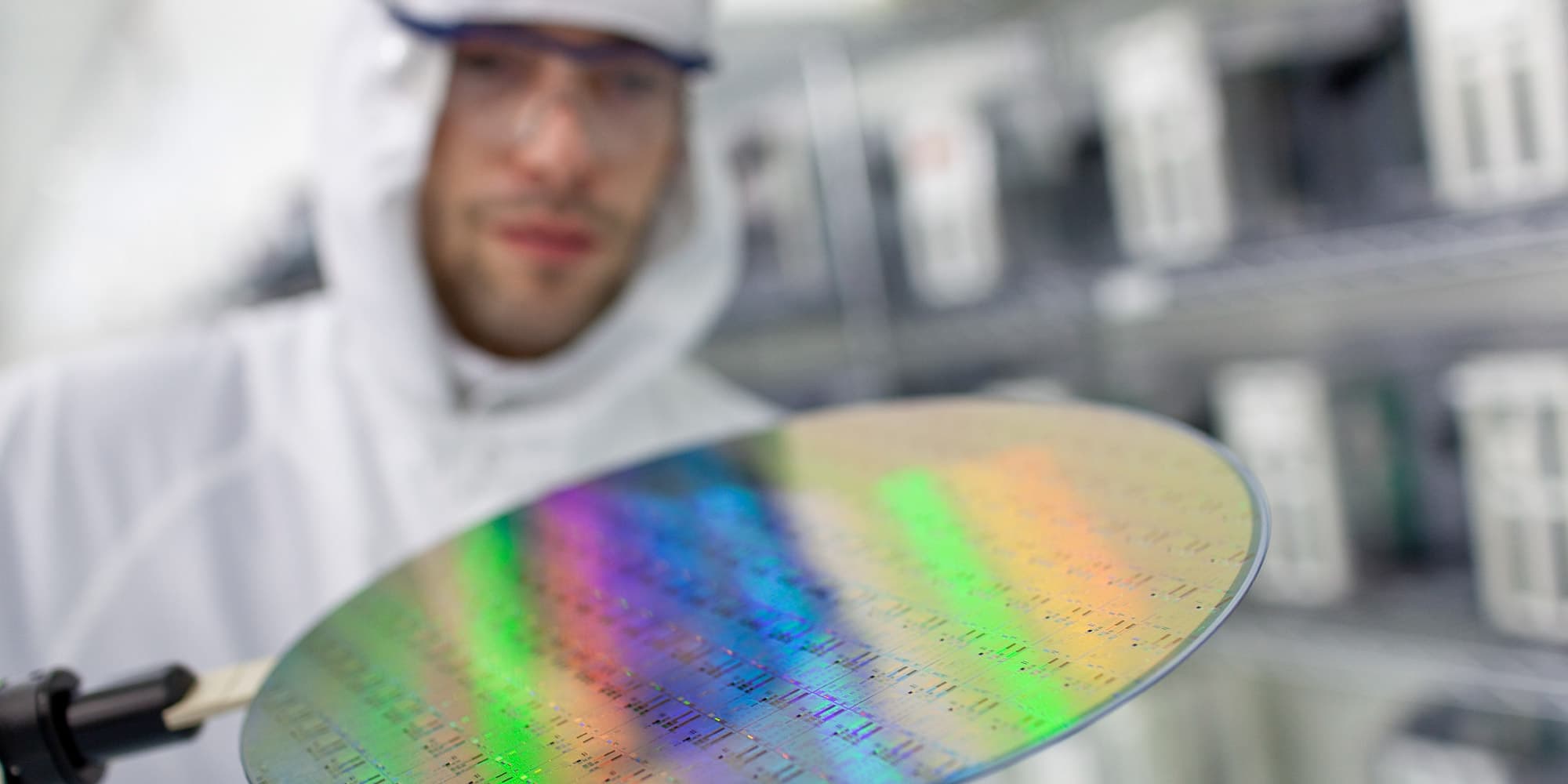
The high-performance compute market will continue to grow because of new application drivers. The 5G rollout will accelerate the already exponential growth of data. This will be combined with growing internet traffic and new data center applications such as supercomputing and high-performance computing-as-a-service. All increasing the demand for high-end CPUs and GPUs inside (cloud) servers. Meanwhile, inside our smartphones, mobile SoCs need to integrate more functionalities in a form-factor-constrained IC.
To achieve these goals, imec collaborates with the entire IC value chain. Constituting one of the world’s largest R&D hubs for next-generation semiconductor research. By building on advanced process steps and materials exploration, fundamental understanding and state-of-the-art fab infrastructure.
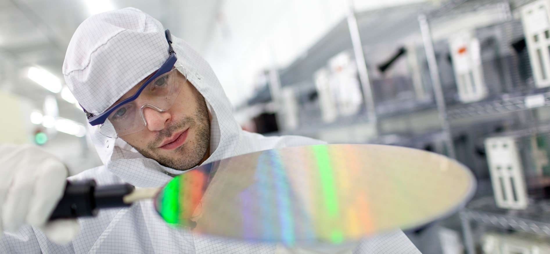
Do you want regular updates on imec’s semiconductor research?
The industry’s largest partner ecosystem for advanced CMOS technology
Imec has set up a unique environment for semiconductor research. A collaboration with the entire value chain, including the world’s major foundries, IDMs, fabless and fablite companies, material and tool suppliers, EDA companies and application developers.
To provide academia and industry early access to the most advanced technology nodes, imec launched its open PDK, embedded in EDA tool suites. Find out more.
It’s a collaboration where all the latest techniques and inventions can be combined and co-optimized. An R&D hub with what’s arguably the world’s densest square mile of expertise, labs and fab infrastructure.

White paper: monolithic microsystems
Elevate your application with advanced functionalities on top of CMOS
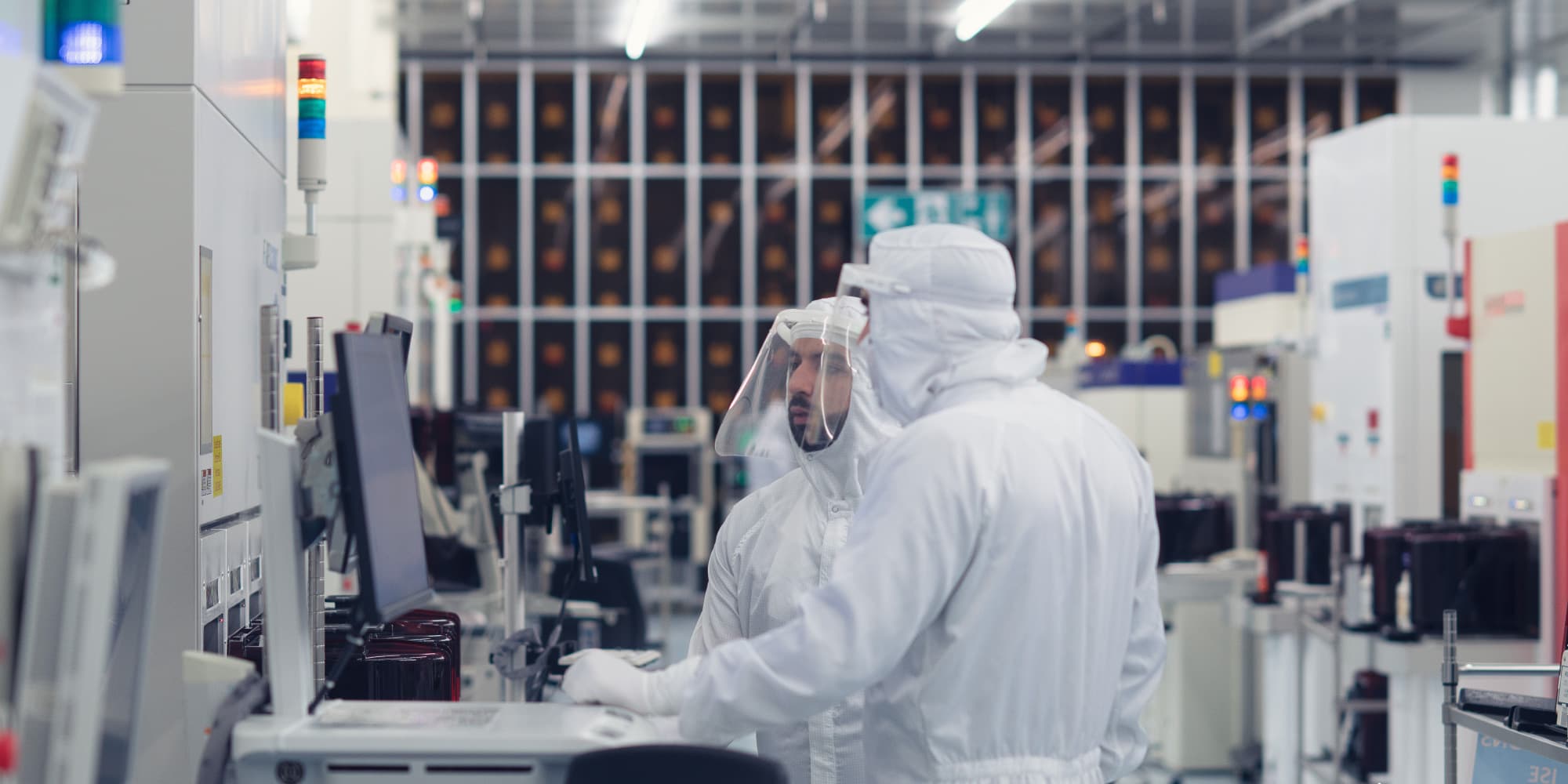
Industry’s most advanced R&D 300mm cleanroom facility
Imec offers a neutral, open innovation R&D platform that involves suppliers profoundly and at an early stage of process step and module development. Thanks to our close partnerships with leading tool and materials suppliers, we can do advanced process development. And offer our partners the industry’s most sophisticated research infrastructure housed within a state-of-the-art 300mm cleanroom.
CMOS technology innovation from a system perspective
Emerging applications such as energy-efficient AI ICs in data centers and edge devices require performance enhancements beyond those from traditional CMOS scaling. One way to achieve this is the simultaneous innovation of system architectures and technology requirements to allow for the most efficient combination of building blocks for the required functionality and performance – or system-technology co-optimization (STCO).
STCO starts by identifying the bottlenecks and challenges in existing systems. Those become the starting point for exploring new system architectures and technologies. The research loop is then closed by evaluating these innovations – and their cohesive integration – through prototypes or other hardware evaluation systems.
Because of its expertise across the technology stack – from semiconductor devices to software – and its prototyping and manufacturing infrastructure and ecosystem, imec offers technology and system companies an STCO innovation sandbox for joint development of next-gen applications.
For imec, STCO is a guiding principle in various research programs such as logic CMOS scaling and Advanced RF. STCO is also being explored at imec USA and imec UK.
Fast cycling between fundamental research, lab probing, and cleanroom enablement
Our scientists and engineers work closely with those of our partners. They’ve set up a fast R&D cycle, feeding the results of fundamental research to the fabs. There, materials and structures are probed and tested for suitability and characteristics.
From the fab, they flow to the cleanroom, looking for faultless manufacturability. The results, measurements and characterization are cycled back into the fundamental research.
Technology centers for advanced CMOS and beyond
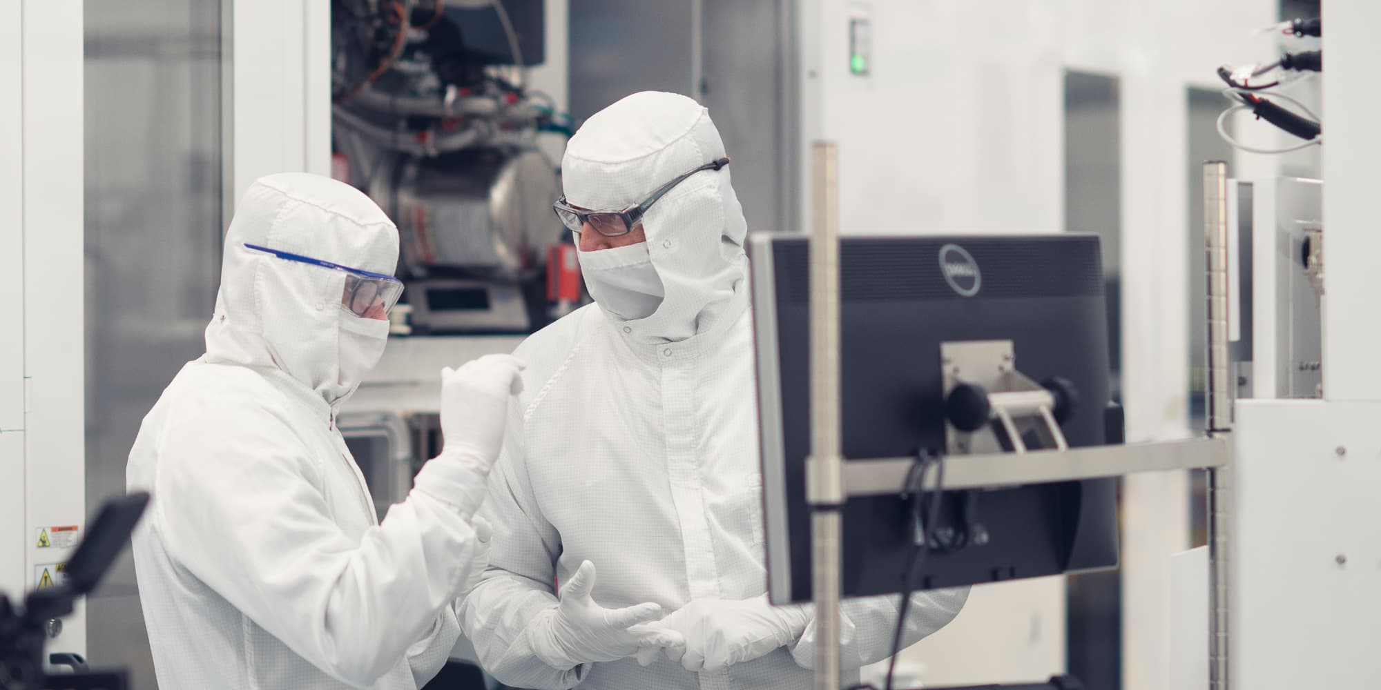
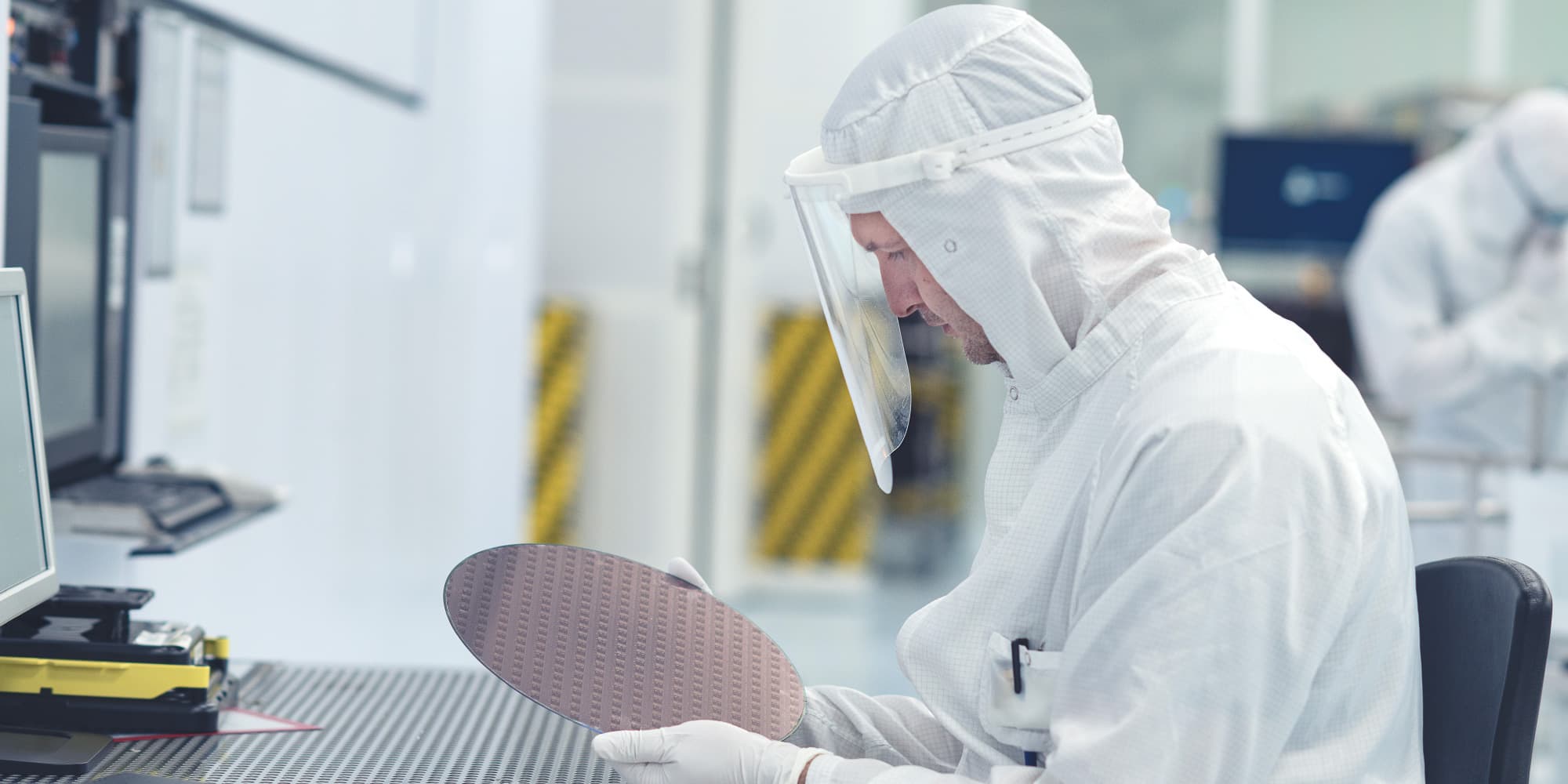
Expertise centers for advanced CMOS and beyond
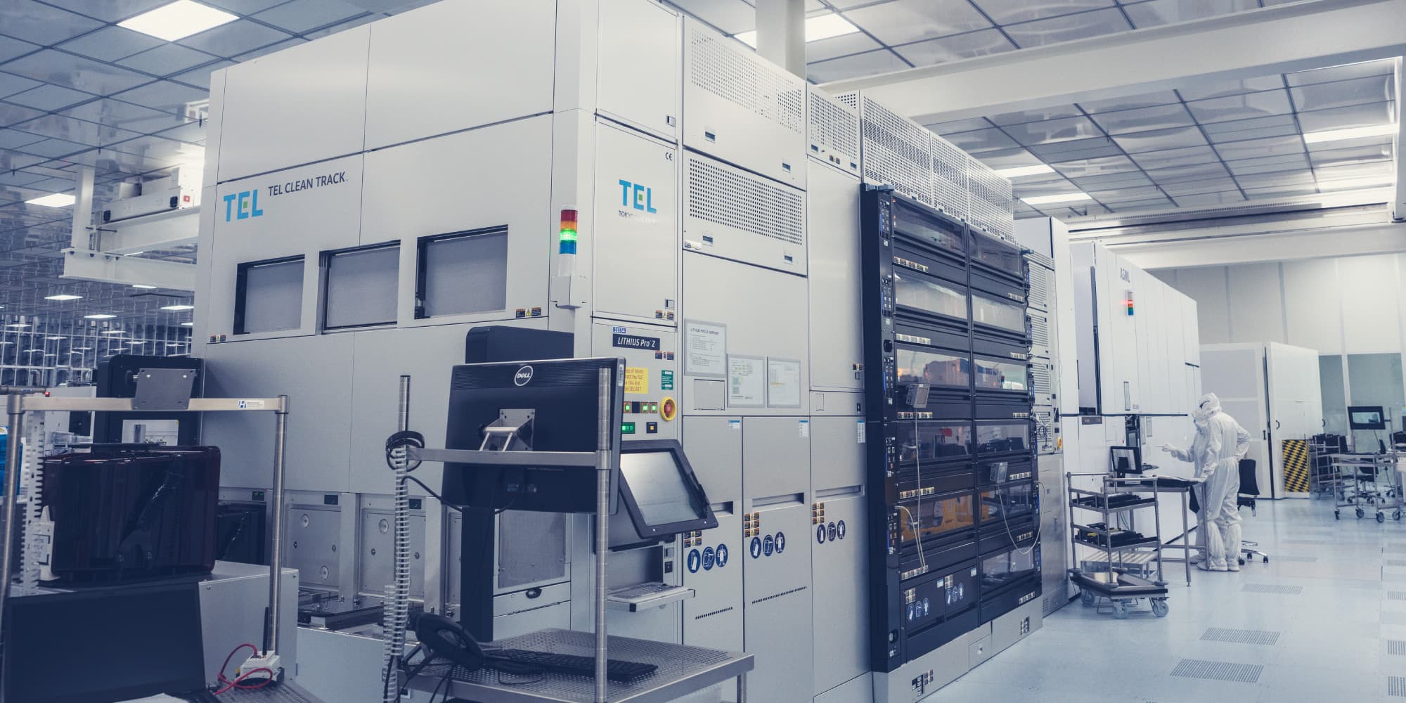
Patterning and process steps
Improved tools and processes are indispensable for new technology nodes.
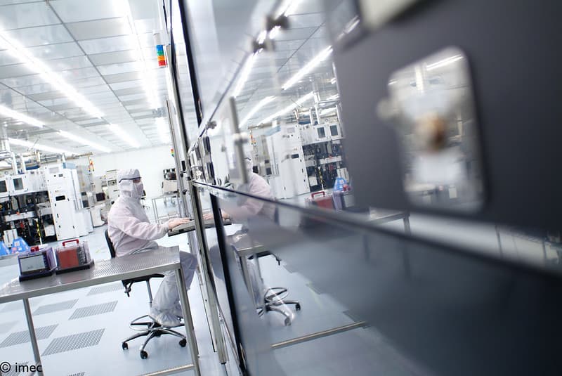
Metrology and characterization
Imec's analytical capabilities support new device architectures.

Reliability testing and modeling
We model and test semiconductor technologies with advanced methods and tools.

Sustainable semiconductor technologies and systems
Imec supports the semiconductor ecosystem's will to make more sustainable choices.
Read more

When does it make sense to move from a monolithic ASIC to a chiplet-based design?
A journey into the benefits, trade-offs and technical implications of moving to chiplets
Read more
Cross-technology co-optimization (XTCO)
A holistic approach to system scaling, connecting AI workload challenges to technology innovations.
Read more
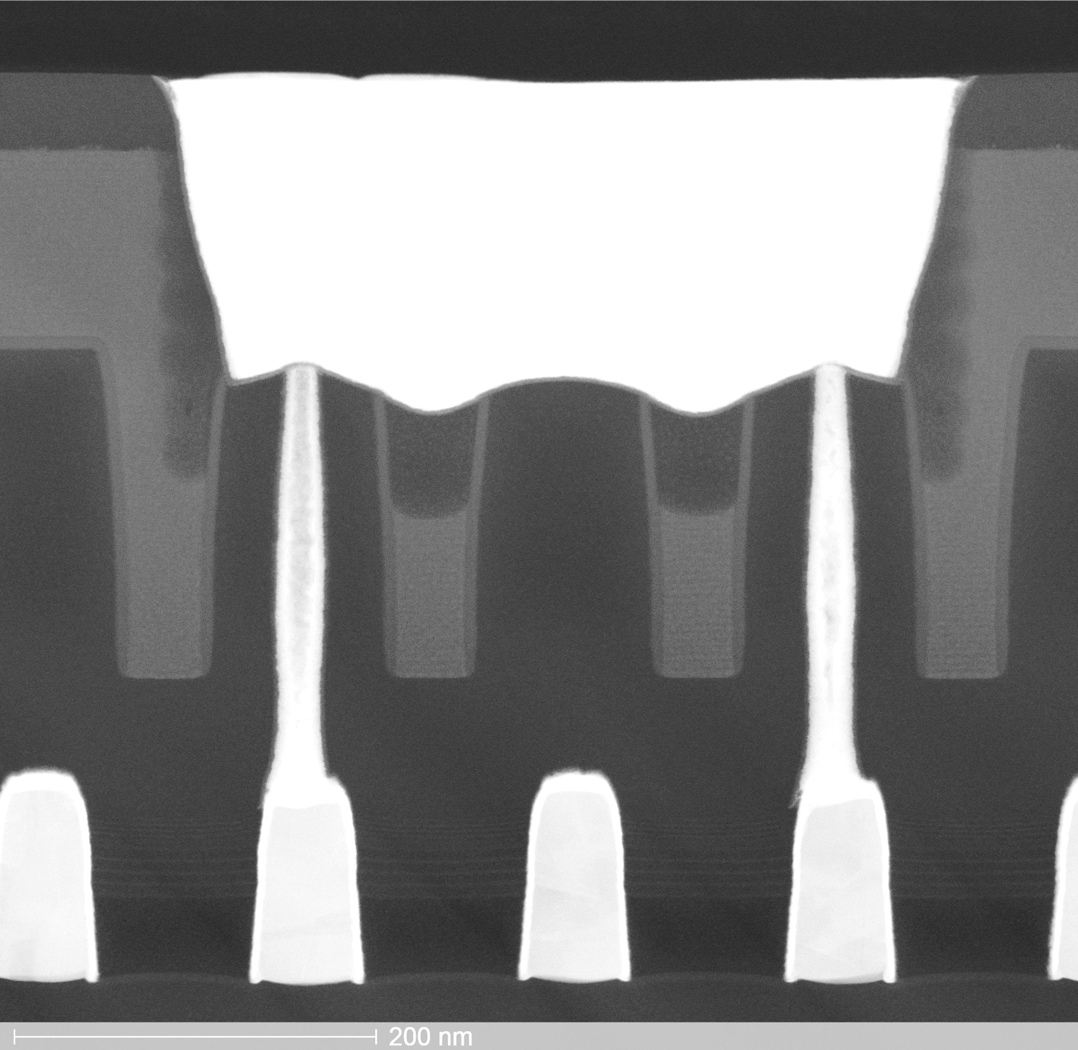
Sony and imec unveil high-density backside connectivity module enabling next-generation 3D chip integration
The new integration approach implements sub-100nm self-aligned through-Si via connections, enabling low-resistance and low-leakage front-to-back connections with good overlay performance
Read moreThe old "relatedjobs" block was not automatically migrated. Related jobs need a split into copy plus VacanciesBlock filtering. Editors should manually revisit this page.
Source content: https://www.imec-int.com/en/expertise/cmos-advanced

Subscribe to our thematic newsletters