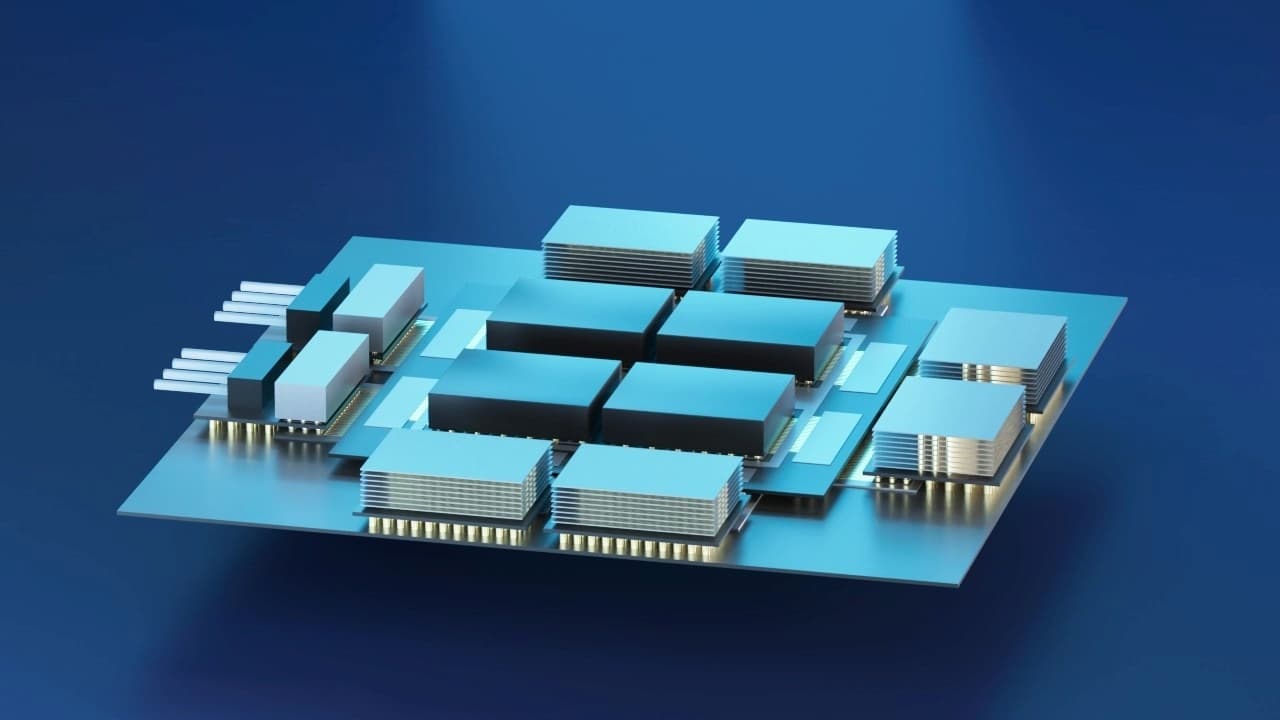
Imec launches the first design pathfinding process design kit for N2 node
The design pathfinding PDK lowers the threshold for academia and industry to access the most advanced semiconductor technologies

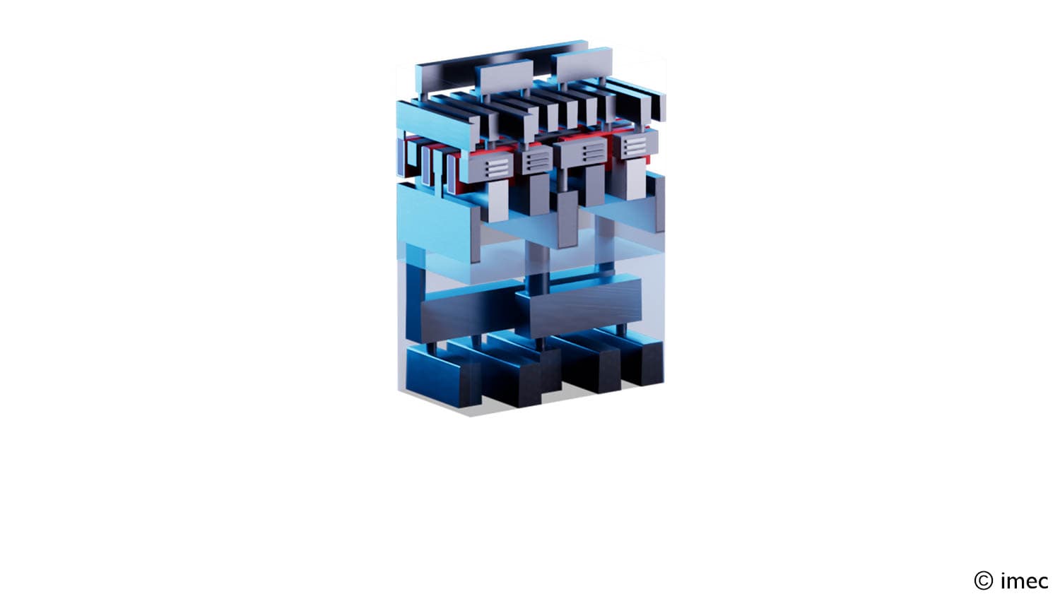
LEUVEN (Belgium), FEBRUARY 16, 2024— This week, at the 2024 IEEE International Solid-State Circuits Conference (ISSCC), imec, a world-leading research and innovation hub in nanoelectronics and digital technologies, launches its design pathfinding process design kit (PDK) with a concomitant training program offered through EUROPRACTICE. The PDK will enable virtual digital designs in imec’s N2 technology, including backside power delivery network. The PDK will be embedded in EDA tool suites, such as from Cadence Design Systems and Synopsys, providing broad access to advanced nodes for design pathfinding, system research and training. This will give academia and industry the tools to train the semiconductor experts of tomorrow and enable the industry to transition their products into next generations technologies through meaningful design pathfinding.
Foundry PDKs give chip designers access to a library of tested and proven components to deliver functional and reliable designs. These are usually available to the ecosystem once the technology reaches a critical level of manufacturability. However, restricted access and the need for NDAs have created a high threshold for academia and industry to access advanced technology nodes during their development. Access to imec N2 PDK will help both academia and commercial companies: “If we want to engage a new generation of chip designers, we must provide them early access to the infrastructure needed to develop their design skills on the most advanced technology nodes. The accompanying training courses will get these designers up to speed as quickly as possible and acquaint them with the most recent technology disruptions such as nanosheet devices and wafer backside technology. The design pathfinding PDK will also help companies to transition their designs to future technology nodes and pre-empt scaling bottlenecks for their products.” says Julien Ryckaert, VP Logic Technologies.
The design pathfinding PDK contains the necessary infrastructure for digital design based on a set of digital standard cell libraries and SRAM IP macros. In the future, the design pathfinding PDK platform will extend to more advanced nodes (e.g. A14). The training program will start early Q2, teaching subscribers the specificities of the N2 technology node and offering hands-on training on digital design platforms using the Cadence and the Synopsys EDA software.
“Nurturing an engineering workforce that is equipped with the necessary technology to develop transformational products is critical to the semiconductor industry,” said Brandon Wang, vice president, technical strategy & strategic partnerships at Synopsys. “Imec’s design pathfinding PDK is an excellent example of how industry partnerships can broaden access to advanced process technology for the current and next generation of designers to accelerate their semiconductor innovation. Our collaboration with imec to deliver a certified, AI-driven EDA digital design flow for its N2 PDK enables design teams to prototype and accelerate the transition to next-generation technologies using a virtual PDK-based design environment.”
“Cadence is committed to working with universities and research institutions to drive innovation and support workforce development for the nano- and microelectronics industry,” said Yoon Kim, VP Cadence Academic Network. “Cadence and imec have a long history of successful collaboration on multiple projects, and the new imec design pathfinding PDK represents a major new milestone for training the next generation of silicon designers. Imec used all the tools in Cadence’s industry leading AI-driven digital and custom / analog full flows to create and validate the Open PDK, ensuring academia and industry partners have access to a complete Cadence flow at the most advanced nodes, enabling them to transition to the next generation of designs seamlessly.”
For inquiries about the design pathfinding PDK, mail to imecpdk@imec.be.
About imec
Imec is a world-leading research and innovation center in nanoelectronics and digital technologies. Imec leverages its state-of-the-art R&D infrastructure and its team of more than 5,500 employees and top researchers, for R&D in advanced semiconductor and system scaling, silicon photonics, artificial intelligence, beyond 5G communications and sensing technologies, and in application domains such as health and life sciences, mobility, industry 4.0, agrofood, smart cities, sustainable energy, education, … Imec unites world-industry leaders across the semiconductor value chain, Flanders-based and international tech, pharma, medical and ICT companies, start-ups, and academia and knowledge centers. Imec is headquartered in Leuven (Belgium), and has research sites across Belgium, in the Netherlands and the USA, and representation in 3 continents. In 2022, imec's revenue (P&L) totaled 846 million euro.
Further information on imec can be found at www.imec-int.com.
Imec is a registered trademark for the activities of imec International (IMEC International, a legal entity set up under Belgian law as a “stichting van openbaar nut”), imec Belgium (IMEC vzw supported by the Flemish Government), imec the Netherlands (Stichting IMEC Nederland), imec Taiwan (IMEC Taiwan Co.), imec India (IMECIndia Private Limited), imec San Francisco (IMEC Inc.) and imec Florida (IMEC USA Nanoelectronics Design Center Inc.).
Discover more


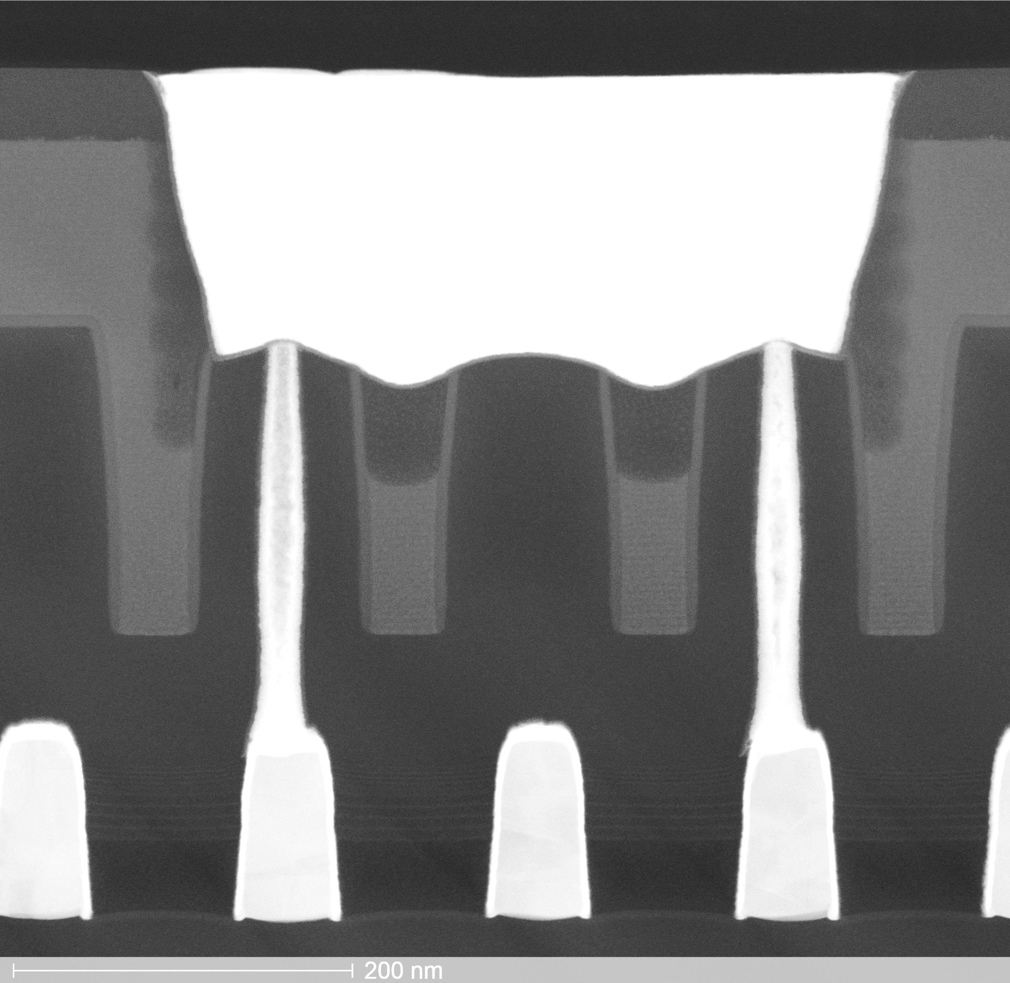
Sony and imec unveil high-density backside connectivity module enabling next-generation 3D chip integration
Read more

ASML, TSMC and imec bring industry-ready 2D-material transistors closer with breakthrough 300mm integration
Read more