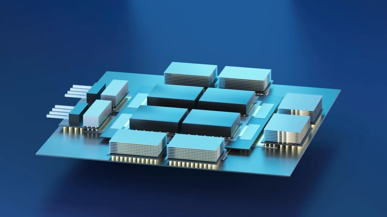
Imec advances 2D-material based device technology beyond state of the art in support of the future logic technology roadmap
Collaboration with leading semiconductor manufacturers pivotal in optimizing the key modules for 2D-material device integration.

LEUVEN (Belgium), December 10, 2025— This week, at the 2025 IEEE International Electron Devices Meeting (IEDM), imec, world-leading research center in advanced semiconductor technologies, presents breakthrough performance of p-type FETs with monolayer WSe2 channels, and improved fab-compatible modules for source/drain contact formation and gate stack integration. These results, achieved through collaborations with leading semiconductor manufacturers, mark a significant advance for 2D-material based technology, which is considered a promising long-term option for extending the logic technology roadmap.
Click here for regular updates on imec's semiconductor research
Replacing Si conduction channels with atomically thin layers made of 2D transition metal dichalcogenides (MX2) promises to enable ultimate gate and channel length scaling, while maintaining good electrostatic channel control and high carrier mobility. Crucial milestones to be achieved include high-quality 2D-material layer deposition, gate stack integration, low-resistance source/drain contact formation, and 300mm fab integration. Also, while most efforts focus on improving n-type devices (with channels made of WS2 or MoS2), more fundamental work is needed on p-type devices, which require different channel materials (such as WSe2).
Gouri Sankar Kar, VP R&D compute and memory device technologies at imec: “At 2025 IEDM, we show in two separate presentations how in-depth collaborations with leading semiconductor manufacturers within imec’s core CMOS Industrial Affiliation Program (IIAP) have enabled breakthroughs in the performance of 2D-material based devices. In both partnerships, combining high-quality 2D material layers provided by the manufacturer with imec’s optimized contact and gate modules played a key role in pushing the technology beyond state of the art.”
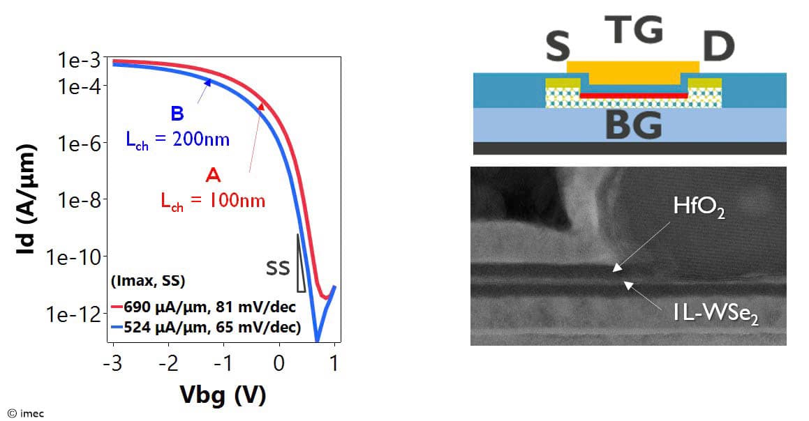
“Depositing the top-gate HfO2 dielectric on top of an MX2 channel requires an additional seed layer to support HfO2 nucleation and growth”, explains Gouri Sankar Kar. “For nFETs, this is solved by creating an AlOx interfacial layer, but this approach is challenging for pFETs due to the different characteristics of the WSe2 channel material as compared to its n-type counterparts. In partnership with TSMC, we started with a synthetic bilayer of WSe2, which was formed by subsequently transferring two high-quality WSe2 monolayers from TSMC on our substrates. We then oxidized the top WSe2 monolayer, converting it into an interfacial layer that successfully supported the deposition of the HfO2 gate oxide. This fab-compatible lab-based integration approach resulted in record performance of our dual-gated pFETs.”
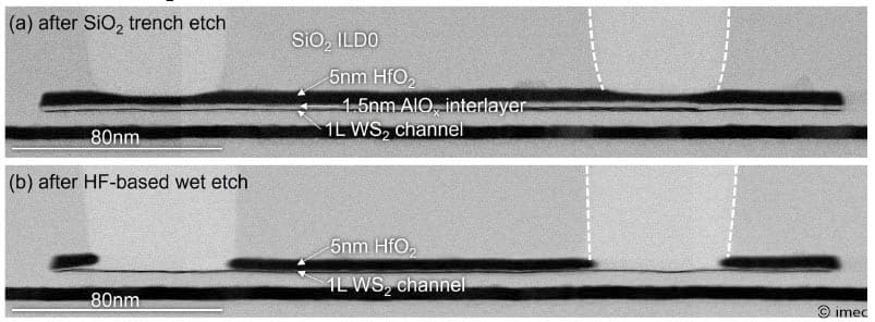
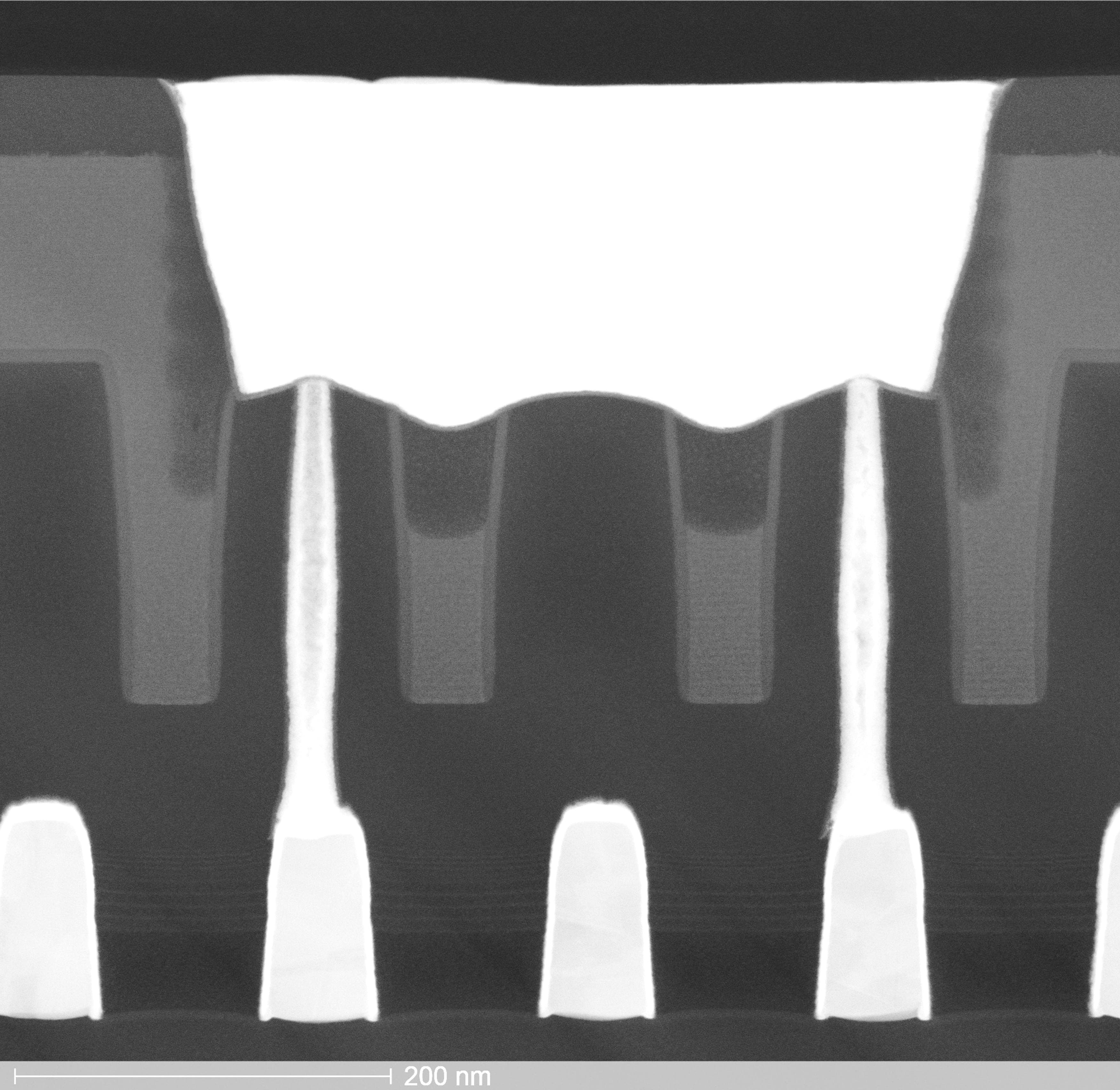
Another presentation highlights the collaboration between imec and Intel in developing 300mm manufacturable modules for source/drain contacts and gate stack integration, for n-type (WS2 and MoS2) and p-type (WSe2) 2D-FETs. “The key innovation consists in applying a selective oxide etch process on Intel’s high-quality 2D material layers, that were capped with an interfacial AlOx layer, an HfO2 layer and a SiO2 layer”, Gouri Sankar Kar explains. “The oxide etch process allowed the formation of fab-compatible damascene-style top contacts – a world first. In addition, during the vertical contact etch process, the interfacial AlOx layer was simultaneously etched laterally, removing AlOx from the channel region. This significantly lowered the top gate’s EOT benefiting the gate’s transfer characteristics.”
This research was funded by the imec IIAP Exploratory Logic program, the 2D-PL pilot line project through Horizon Europe (101189797) and Horizon 2020 (952792) grant agreements.
About imec
Imec is a world-leading research and innovation hub in advanced semiconductor technologies. Leveraging its state-of-the-art R&D infrastructure and the expertise of over 6,500 employees, imec drives innovation in semiconductor and system scaling, artificial intelligence, silicon photonics, connectivity, and sensing.
Imec’s advanced research powers breakthroughs across a wide range of industries, including computing, health, automotive, energy, infotainment, industry, agrifood, and security. Through IC-Link, imec guides companies through every step of the chip journey - from initial concept to full-scale manufacturing - delivering customized solutions tailored to meet the most advanced design and production needs.
Imec collaborates with global leaders across the semiconductor value chain, as well as with technology companies, start-ups, academia, and research institutions in Flanders and worldwide. Headquartered in Leuven, Belgium, imec has research facilities in Belgium, across Europe and the USA, and representation on three continents. In 2024, imec reported revenues of €1.034 billion.
For more information, visit www.imec-int.com
The imec group holds a global trademark portfolio, including word marks and combined figurative registered and unregistered trademarks, across national, regional, and international territories. Its lawful use requires prior written consent of IMEC in compliance with the IMEC branding guidelines, which may be updated periodically. The latest version is available upon written request.
Discover more

Sony and imec unveil high-density backside connectivity module enabling next-generation 3D chip integration
Read more

ASML, TSMC and imec bring industry-ready 2D-material transistors closer with breakthrough 300mm integration
Read more