Imec mitigates thermal bottleneck in 3D HBM-on-GPU architectures using a system-technology co-optimization approach
Holistic system-technology co-optimization (STCO) approach key in reducing peak GPU and HBM temperatures under AI workloads while enhancing performance density of future GPU-based architectures

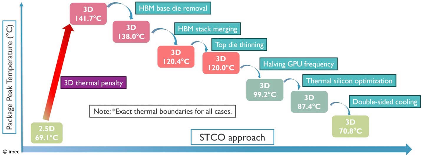
LEUVEN (Belgium), December 8, 2025— This week, at the 2025 IEEE International Electron Devices Meeting (IEDM), imec, world-leading research center in advanced semiconductor technologies, presents the first thermal system-technology co-optimization (STCO) study of 3D HBM-on-GPU (high-bandwidth memory on graphical processing unit), a promising compute architecture for next-gen AI applications. By combining technology and system-level mitigation strategies, peak GPU temperatures could be reduced from 141.7°C to 70.8°C under realistic AI training workloads – on par with current 2.5D integration options. The result demonstrates the strength of combining cross-layer optimization (i.e., co-optimizing the knobs at all the different abstraction layers) with broad technological expertise, a combination that is unique to imec.
Click here for regular updates on imec’s semiconductor research
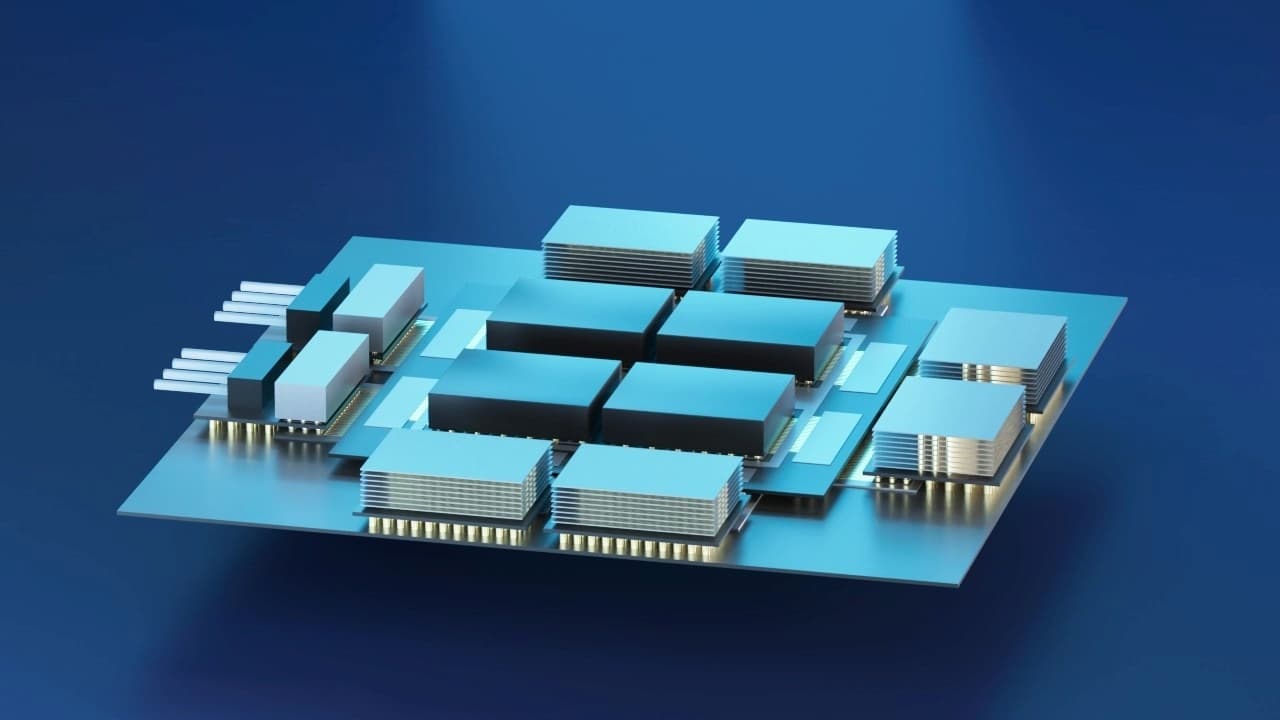
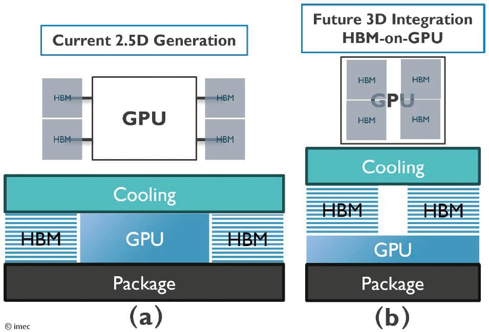
Integrating high bandwidth memory (HBM) stacks directly on top of graphical processing units (GPUs) offers an attractive approach for building next-gen compute architectures for data-intensive AI workloads. This 3D HBM-on-GPU promises a huge leap forward in compute density (with four GPUs per package), memory per GPU, and GPU-memory bandwidth compared to current 2.5D integration options where HBM stacks are placed around (one or two) GPUs on a silicon interposer. However, the aggressive 3D integration approach is prone to thermal issues because of higher local power density and vertical thermal resistance.
At 2025 IEDM, imec presents the first comprehensive thermal simulation study of 3D HBM-on-GPU integration that not only identifies thermal bottlenecks but also proposes strategies to increase the architecture’s thermal feasibility. Imec researchers show how co-optimizing technology and system-level thermal mitigation approaches can reduce peak GPU temperatures from 141.7°C to 70.8°C under realistic AI training workloads.
The model assumes four HBM stacks – each consisting of twelve hybrid-bonded DRAM dies – placed directly on top of a GPU using microbumps. Cooling is provided on top of the HBMs. Power maps derived from industry-relevant power profiles are applied to identify local hotspots and compare them to a 2.5D baseline. Without thermal mitigation strategies, the 3D model yields a peak GPU temperature of 141.7°C – far too high for GPU and HBM operation – while the 2.5D integration benchmark peaks at a workable 69.1°C under the same cooling conditions. We used these data as a starting point to evaluate the joint impact of technology and system-level thermal mitigation strategies. Technology-level strategies include, among others, HBM stack merging and thermal silicon optimization. On the system-level side, we assessed the impact of double-sided cooling as well as GPU frequency scaling.
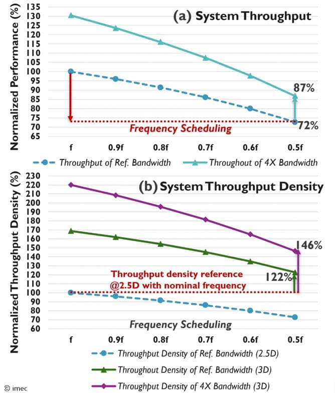
James Myers, System Technology Program Director at imec: “Halving the GPU core frequency brought the peak temperature from 120°C to below 100°C, achieving a key target for the memory operation. Although this step comes with a 28% workload penalty (i.e., a slowdown of AI training steps), the overall package outperforms the 2.5D baseline thanks to a higher throughput density offered by the 3D configuration. We are currently using this approach to study other GPU/HBM configurations (e.g., placing GPUs on top of HBMs), anticipating future thermal constraints.”
Julien Ryckaert, Vice President Logic Technologies at imec: “This is also the first time that we demonstrate the capabilities of imec’s cross-technology co-optimization (XTCO) program in building more thermally robust compute systems. XTCO was launched in 2025 to efficiently align imec’s technology roadmaps with key industry system scaling challenges and is built on four critical system level pillars: compute density, power delivery, thermal, and memory density and bandwidth. It combines our STCO/DTCO mindsets with imec’s broad technology expertise – a unique combination that is of great value in addressing the growth and diversification of compute system demands. We invite companies from within the entire semiconductor ecosystem, including fabless and system companies, to join our XTCO program and collaboratively resolve critical system scaling bottlenecks.”
About imec
Imec is a world-leading research and innovation hub in advanced semiconductor technologies. Leveraging its state-of-the-art R&D infrastructure and the expertise of over 6,500 employees, imec drives innovation in semiconductor and system scaling, artificial intelligence, silicon photonics, connectivity, and sensing.
Imec’s advanced research powers breakthroughs across a wide range of industries, including computing, health, automotive, energy, infotainment, industry, agrifood, and security. Through IC-Link, imec guides companies through every step of the chip journey - from initial concept to full-scale manufacturing - delivering customized solutions tailored to meet the most advanced design and production needs.
Imec collaborates with global leaders across the semiconductor value chain, as well as with technology companies, start-ups, academia, and research institutions in Flanders and worldwide. Headquartered in Leuven, Belgium, imec has research facilities in Belgium, across Europe and the USA, and representation on three continents. In 2024, imec reported revenues of €1.034 billion.
For more information, visit www.imec-int.com
The imec group holds a global trademark portfolio, including word marks and combined figurative registered and unregistered trademarks, across national, regional, and international territories. Its lawful use requires prior written consent of IMEC in compliance with the IMEC branding guidelines, which may be updated periodically. The latest version is available upon written request.