Imec first to demonstrate conductor films on 300mm wafers with lower resistivity than Cu and Ru
The results motivate the continued search for binary and ternary alloys to replace Cu and Ru in advanced interconnect metallization schemes
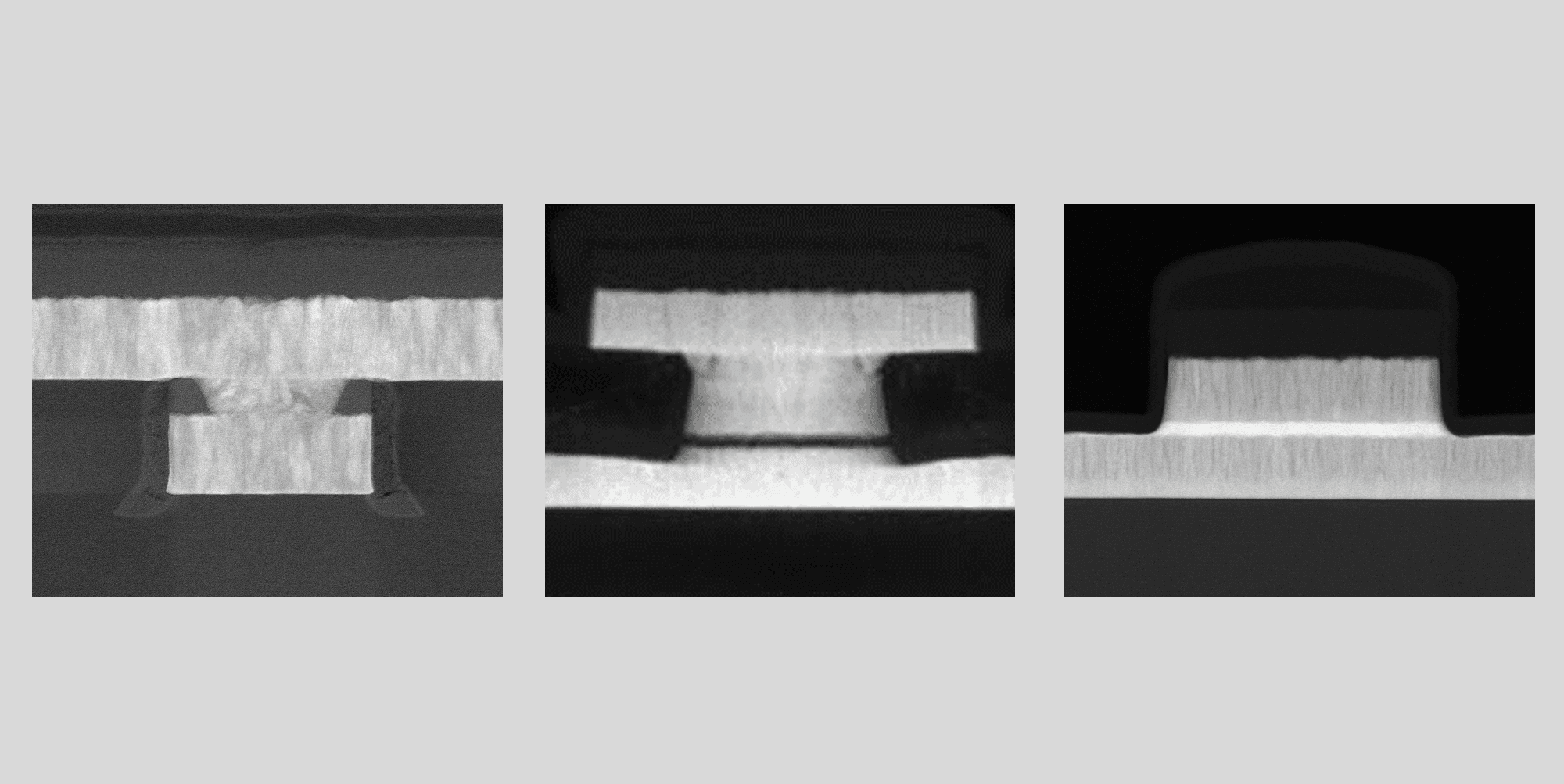
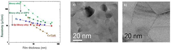
LEUVEN (Belgium), MAY 23, 2023— This week, at the 2023 IEEE International Interconnect Technology Conference (2023 IEEE IITC), imec, a world-leading research and innovation hub in nanoelectronics and digital technologies, provides the first experimental evidence that the resistivity of a thin conductor film on a 300mm Si wafer can be lower than that of Cu and Ru, which are currently used in interconnect metallization schemes. For example, a resistivity as low as 11.5µWcm was measured for a NiAl binary alloy of 7.7nm thickness, obtained after grain size engineering. The results mark a milestone towards enabling low-resistive interconnect with line widths below 10nm.
To keep pace with the continuing device scaling, the width of the most critical interconnect lines in state-of-the-art logic and memory chips soon approaches 10nm. At these small dimensions, the resistivity of Cu increases dramatically, and its reliability degrades. This has forced the interconnect community to identify alternatives to Cu metallization. While the focus was initially on elemental metals, the search has been extended to binary and ternary ordered intermetallics – initiated by imec at the 2018 IITC conference.
Imec set up a unique ab-initio-based methodology to select and rank the most promising materials, using the product of the bulk resistivity and the mean free path of the charge carriers (r0 x l) as one of the main figures of merit. This theoretical assessment was the starting point for further experimental work on 300mm wafers. Zsolt Tőkei, fellow and program director of nano-interconnects at imec: “To better understand and model the resistivity behavior of the selected binary alloys at small dimensions, we introduce at the 2023 IEEE IITC conference an effective resistivity, which considers composition variation and the effects of order and disorder. Further analysis revealed that the resistivity of thin films of binary alloys is dominated by grain boundary scattering due to the small grain sizes inherently present in thin conductor films, whereas disorder contributes for thicker films as well.”
For the case study of stoichiometric NiAl, a resistivity as low as 11.5µ Ohm cmwas measured on a 7.7nm thin film, which is 23% lower than Cu. This was achieved after depositing a 50nm thick large-grain NiAl film on a Ge epi-layer at back-end-of-line (BEOL) compatible temperatures, followed by thinning experiments. These experiments preserve a larger grain size (45.7nm) and hence reduce the contribution of grain boundary scattering to resistivity. Zsolt Tőkei: “The experimental existence of low-resistive thin conductor films on 300mm wafers motivates us to continue our search for binary and ternary alloys. At the same time, we investigate the composition control of the alloys and their integration compatibility with future metallization schemes that will likely be based on subtractive etch.”
At 2023 IEEE IITC, imec has 10 oral presentations addressing the main challenges in interconnect scaling. Besides two papers on alternative metals exploration – including one invited contribution – the papers highlight work on semi-damascene metallization, reliability, thermal impact of advanced interconnect stacks, middle-of-line metallization schemes, and more.
About imec
Imec is a world-leading research and innovation center in nanoelectronics and digital technologies. Imec leverages its state-of-the-art R&D infrastructure and its team of more than 5,500 employees and top researchers, for R&D in advanced semiconductor and system scaling, silicon photonics, artificial intelligence, beyond 5G communications and sensing technologies, and in application domains such as health and life sciences, mobility, industry 4.0, agrofood, smart cities, sustainable energy, education, … Imec unites world-industry leaders across the semiconductor value chain, Flanders-based and international tech, pharma, medical and ICT companies, start-ups, and academia and knowledge centers. Imec is headquartered in Leuven (Belgium), and has research sites across Belgium, in the Netherlands and the USA, and representation in 3 continents. In 2022, imec's revenue (P&L) totaled 846 million euro.
Further information on imec can be found at www.imec-int.com.
Imec is a registered trademark for the activities of imec International (IMEC International, a legal entity set up under Belgian law as a “stichting van openbaar nut”), imec Belgium (IMEC vzw supported by the Flemish Government), imec the Netherlands (Stichting IMEC Nederland), imec Taiwan (IMEC Taiwan Co.), imec China (IMEC Microelectronics (Shanghai) Co. Ltd.), imec India (IMEC India Private Limited), imec San Francisco (IMEC Inc.) and imec Florida (IMEC USA Nanoelectronics Design Center Inc.).
Discover more

A double world-first: integrating lithium niobate and lithium tantalate modulators on silicon photonics through micro-transfer printing
Read more
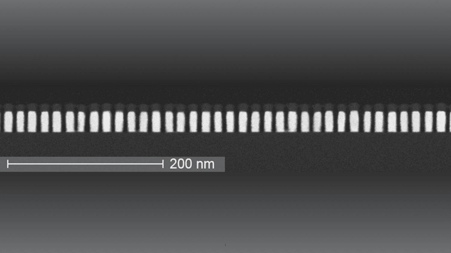
Imec demonstrates 16nm pitch Ru lines with record-low resistance obtained using a semi-damascene integration approach
Read more