Europe’s pilot line to enable future compute systems
Accelerating beyond-2nm chip innovation across Europe

In short
With traditional scaling metrics struggling to meet emerging tech demands, rethinking compute systems is essential.
The NanoIC pilot line, focused on innovation through collaboration of advanced logic, novel memories, and advanced interconnects, aims to fulfill the European Chips Act's vision for leadership and competitiveness in global semiconductor innovation.
This article was previously published in Nature Reviews electrical engineering and adapted to a Q&A in SEMI.
To bridge the gap between research innovation and commercialization in the semiconductor industry, a robust lab-to-fab conduit is essential. Europe is positioning itself at the forefront with the NanoIC pilot line, which aims to mature specific semiconductor technologies to foster innovation in computing system architectures. Aligned with the European Chips Act, NanoIC pilot line seeks to enhance Europe’s leadership in critical markets such as computing, communication, automotive, energy, and health. The goal is to get European companies to lead semiconductor innovation, rather than merely consuming it.
The project, hosted by imec, is one of four innovative semiconductor pilot lines approved by the Chips Joint Undertaking (Chips JU), alongside with i) advanced fully depleted silicon on insulator technologies (led by CEA-Leti, France); ii) advanced heterogeneous system integration and assembly (led by Fraunhofer, Germany); and iii) advanced semiconductor devices based on wide bandgap materials (led by Tampere University, Finland).
Specifically, NanoIC pilot line is set to provide a leading-edge beyond 2nm system-on-chip (SoC) pilot line for advanced logic, memory, and interconnect technologies. The project focuses on large-scale capacity building and innovation support, providing the entire semiconductor ecosystem access to advanced technologies in logic, memory and interconnects. This initiative will help maintain European competitiveness across the entire semiconductor value chain: from materials, equipment, processes, devices to design and systems.
Meet the NanoIC consortium
The successful implementation of the NanoIC pilot line relies on a consortium led by imec, alongside CEA-Leti, Fraunhofer-Gesellschaft (FhG), VTT Technical Research Center of Finland, Tyndall National Institute, and the Center for Surface Science and Nanotechnology of the University POLITEHNICA of Bucharest. These institutions will collaborate to bring together a wealth of knowledge and state-of-the-art facilities to bolster European technological leadership and innovation in semiconductor technologies. NanoIC pilot line is supported by the Flemish Government, other participating states, and the Chips Joint Undertaking of the EU Chips Act.
Renowned for its research in nanoelectronics and digital technologies, imec (Belgium) provides extensive R&D infrastructure and deep semiconductor technology expertise. The research fab FhG (Germany) combines the strengths of multiple national research institutions to support micro- and nanoelectronics, the largest of its kind in Europe. In the same field, CEA-Leti (France) bridges academic research and industrial production with its advanced R&D capabilities. Research center VTT (Finland) specializes in sustainable and digital technologies, utilizing its Micronova cleanroom facility. Tyndall (Ireland) offers experience in semiconductor research and ICT, including advanced fabrication capabilities and CSSNT-UPB (Romania) contributes advanced equipment and research expertise from its state-of-the-art nanotechnology labs.
Next big leap in semiconductor technology
Since the early 1990s, complementary metal oxide semiconductor (CMOS) logic, static random-access memory (SRAM), and dynamic RAM (DRAM) scaling have revolutionized the electronics industry, striking a balance between performance, energy efficiency, and affordability. The SoC paradigm enabled by general-purpose CMOS logic technology has led to increasingly complex systems, integrating an ever-growing number of transistors on a single chip. However, as the demands of new applications like machine learning, augmented reality/virtual reality, or autonomous vehicles, intensify, the need to rethink compute systems is pressing. Moreover, the diminishing returns of traditional scaling metrics (such as power-performance-area-cost) require innovative approaches to advance technology.
The transition from fin field-effect transistors (finFETs) to gate-all-around nanosheet devices, marked a notable advancement in CMOS device technology. FinFETs have underpinned the CMOS technology from the 22nm to the 3nm node. However, starting at the 2nm node, which is expected to enter production next year, nanosheet devices will be introduced. Nanosheet class of devices, including variants like Forksheet devices, are anticipated to drive scaling and performance through three generations (2nm, A14, A10) [1]. Following this, complementary FET (CFET) architectures are projected to be introduced around 2031 at the A7 node, representing another major inflection point in CMOS device design [2]. This progression demands extensive research into new materials, process modules, equipment and advanced patterning capabilities using high numerical aperture extreme ultraviolet (high NA EUV) lithography.
Looking into memory innovations, as SRAM scaling slows, exploring novel dense embedded memory concepts becomes imperative. Technologies such as spin orbit torque magnetic RAM (SOT-MRAM) and 2-transistor 0-capacitor (2T0C) embedded DRAM using deposited semiconductors like Indium Gallium Zinc Oxide are promising. In parallel, developing a 3D memory platform to explore future novel memory options – to augment SRAM and DRAM - is essential to address memory capacity and memory bandwidth challenges from new workloads.
Chip-to-chip lateral interconnects (also referred to as 2.5D or interposer technologies) and chip-to-chip vertical interconnects (3D technologies) have been used to address the memory capacity and bandwidth challenges, or to partition SoC functions into separate die [3]. Since the mid-2010s, advances in chip-to-chip electrical interconnects have included pitch scaling of micro-bumps and Cu hybrid bonding, which enable fine-grained partitioning of SoC functions. Additionally, advances in Si-photonics-based optical interconnects and 3D interconnect-enabled co-packaging offer high-bandwidth and low-power optical connectivity over shorter distances. The rise of chiplet architectures and standardization will drive demand for low-cost, wafer-level tight-pitch interconnect technologies like Cu/polymer redistribution layers. A future high-performance compute system should leverage and integrate seamlessly these different innovations (Figure 1).
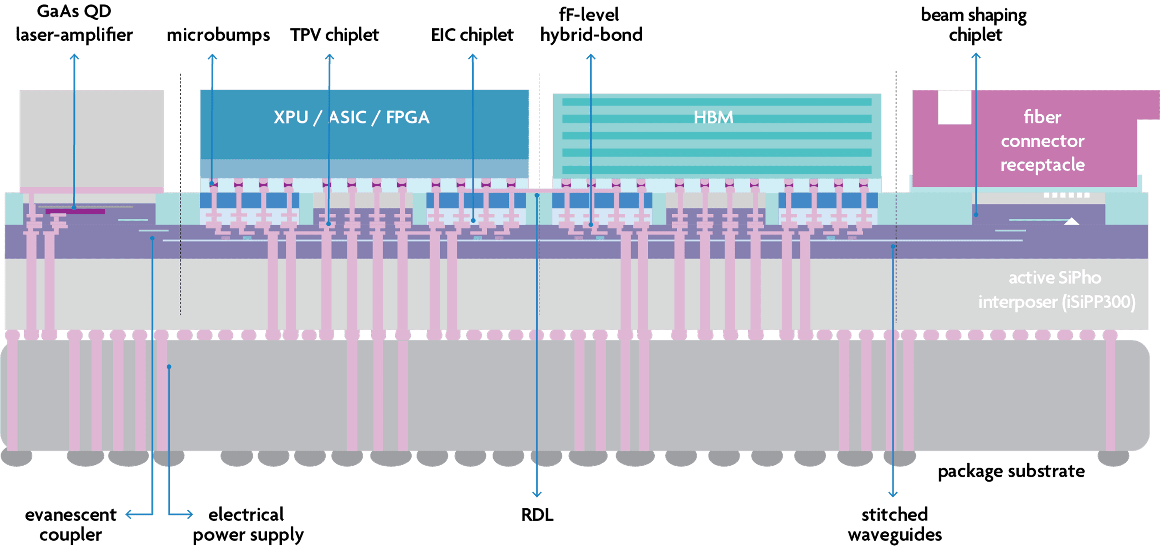
Building blocks of future compute systems
Advanced logic, novel memories, and advanced interconnects will be at the heart of the NanoIC pilot line, that will develop baselines using new equipment and research into new materials and modules. The approach includes maturing integration baseline flows for repeatability, variability, and defectivity improvements. Sustainable process development will be a priority during the module research phase, integrating environmental considerations from the outset.
The logic flows will be based on a nanosheet baseline, supporting A14 and A10 logic nodes, and a CFET baseline, including High NA EUV patterning and targeting A7 and beyond logic nodes. Advanced memory technology flows such as SOT-MRAM and embedded DRAM based on deposited semiconductors will also be developed. Advanced interconnects will be matured to support die to wafer hybrid bonding connectivity of < 3 µm pitch and a fine-pitch re-distribution layers at < 1 µm line/space to enable chiplet architectures. To obtain integration of optical interconnects at wafer level, integrated III-V lasers with die to wafer connectivity on optical interposers will be developed.
These innovative technologies will be accessible to designers through research process design kits (PDKs) for system exploration and prototyping PDKs for system demonstrators. The PDKs will enable virtual prototyping of new system architectures as well as prototyping using foundry logic wafers.
The road ahead
As the NanoIC pilot line progresses, it will continue to build upon the foundational work established by precursor initiatives of Chips JU like the Electronic Components and Systems for European Leadership (ECSEL), and Key Digital Technologies (KDT) as well as regional government-funded projects. This collaborative effort promises to deliver marked benefits across various sectors. Integrated device manufacturers and foundries will leverage the nanosheet and CFET baselines to explore new module and performance enhancement options. Equipment and materials suppliers, both European and global, will collaborate to enable the advanced baselines to test and refine new tools and processes. Furthermore, start-ups, universities, and design companies will have access to research PDKs for system pathfinding and hybrid PDKs for system prototyping. This will not only strengthen the European semiconductor ecosystem but also drive growth among European entities in the microelectronics sector.
In summary, the NanoIC pilot line represents a strategic effort to bridge the gap between cutting-edge research and commercial application in the semiconductor industry. The project underscores Europe’s commitment to innovation, competitiveness, and sustainable growth in an increasingly digital world. By advancing technologies, fostering collaboration, and emphasizing sustainability, the project aims to consolidate Europe’s leadership in the global semiconductor market.
The acquisition and operation of the Chips JU pilot line are jointly funded by the Chips Joint Undertaking, through the European Union’s Digital Europe and Horizon Europe programs, as well as by the participating states.
References
Samavedam, S.B. et al. Future Logic Scaling: Towards Atomic Channels and Deconstructed Chips. IEEE International Electron Devices Meeting (IEDM), San Francisco, CA, USA, 1.1.1-1.1.10 (2020). doi: 10.1109/IEDM13553.2020.9372023
Horiguchi, N. et al. 3D Stacked Devices and MOL Innovations for Post-Nanosheet CMOS Scaling. International Electron Devices Meeting (IEDM), San Francisco, CA, USA, 1-4 (2023). doi: 10.1109/IEDM45741.2023.10413701
Beyne, E. The 3-D Interconnect Technology Landscape, IEEE Design & Test 33, no. 3, 8-20 (2016). doi: 10.1109/MDAT.2016.2544837
Related links
Authors

Sri Samavedam
Sri Samavedam is senior vice president of CMOS technologies at imec since August 2019. His responsibilities include programs in logic, memory, photonics and 3D integration. Prior to that, he was senior director of technology development at GlobalFoundries in Malta, NY. There, he led the qualification of 14nm FinFET technology and derivatives into volume production and early development of 7nm CMOS. He began his research career at Motorola in Austin, TX, working on strained silicon, metal gates, high-k dielectrics and fully-depleted SOI devices. He holds a Ph.D. in Materials Science and Engineering from MIT and a masters from Purdue University.

Jo De Boeck
Jo De Boeck joined the company in 1991 after earning his Ph.D. from KU Leuven. He has held various leadership roles, including head of the Microsystems division and CTO. He is also a part-time professor at KU Leuven and was a visiting professor at TU Delft. Jo oversees imec's strategic direction and is a member of the Executive Board.