A technology platform for thermally stable DRAM peripheral transistors
Imec proposes different material and integration options in response to the evolving needs of the DRAM periphery

In short
Dynamic random-access memory (DRAM) chips contain many other transistors besides the access transistor to enable full operation of the DRAM memory.
These peripheral transistors must meet stringent requirements which preclude a ‘copy-paste’ of regular logic transistor process flows.
One critical requirement imposed by present DRAM chip architectures is the ability of the periphery to withstand thermal treatments at 550-600°C and above.
Imec pioneered different generations of thermally stable peripheral transistor technology – from planar high-k/metal-gate transistors to FinFETs.
DRAM: the main memory in traditional compute architectures
For decades, compute architectures have relied on dynamic random-access memory (DRAM) as their main memory, providing temporary storage from which processing units retrieve data and program code. The high-speed operation, large integration density, cost-effectiveness, and excellent reliability have contributed to the widespread adoption of DRAM technology in many electronic devices.
The DRAM bit cell, i.e., the element that stores one bit of information, has a very basic structure. It consists of one capacitor (1C) and one transistor (1T) integrated close to the capacitor. While the capacitor’s role is to store a charge, the transistor is used to access the capacitor, either to read how much charge is stored or to store a new charge. The 1T-1C bit cells are arranged in arrays containing word and bit lines, and the word line is connected to the transistors’ gate, which controls access to the capacitor. The memory state can be read by sensing the stored charge on the capacitor via the bit line.
Over the years, the memory community introduced subsequent generations of DRAM technology, enabled by continuous bit-cell density scaling. Current DRAM chips belong to the ‘10nm class’ (denoted as D1x, D1y, D1z, D1α...), where the half pitches of the active area in the memory cell array range from 19 down to 10nm. The AI-driven demand for better performing and larger capacity DRAM is propelling R&D into beyond-10nm generations. This requires innovations in capacitors, access transistors, and bit cell architectures. Examples of such innovations are high-aspect ratio pillar capacitors, the move from saddle-shaped (FinFET-based) access transistors to vertical-gate architectures, and the transition from 6F2 to 4F2 cell designs (F being the minimum feature size for a given technology node) [1].
A closer look inside a planar 1T-1C DRAM chip: the peripheral circuit
To enable full functionality of the DRAM chip, several other transistors are needed besides the access transistors. These additional transistors play a role in, for example, the address decoder, sense amplifier, or output buffer function. They are called DRAM peripheral transistors and are traditionally fabricated next to the DRAM memory array area [2].
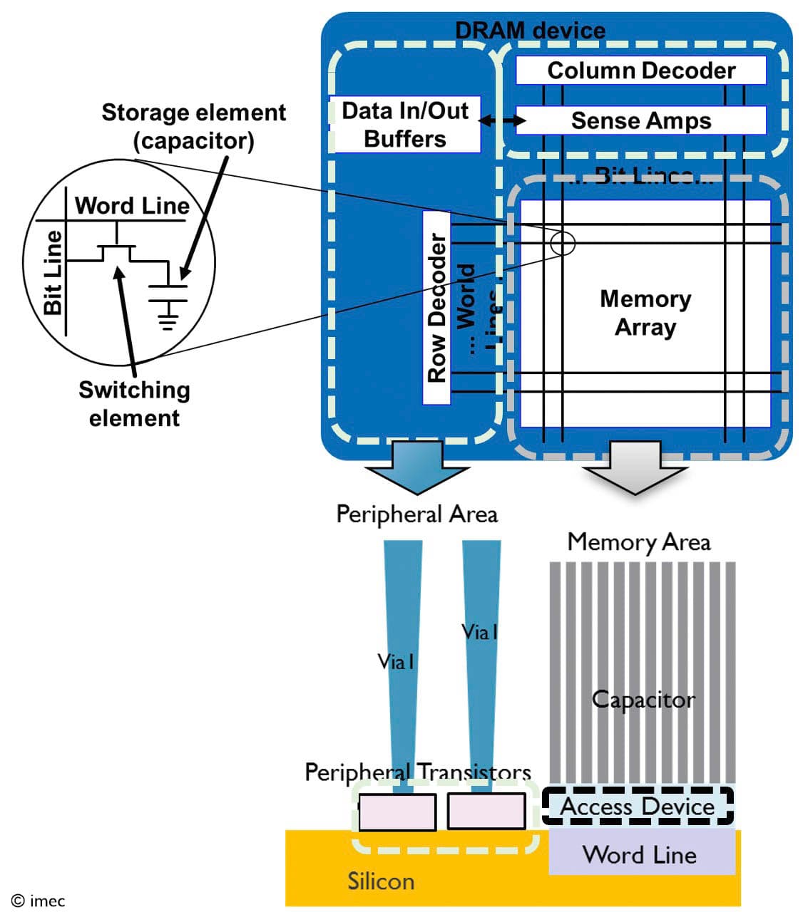
DRAM peripheral transistors can be grouped into three main categories. The first category is regular logic transistors: digital switches that are repeatedly turned on and off. The second category is sense amplifiers – analog types of transistors that sense the difference in charge between two bit cells. A small positive change is amplified into a high voltage (representing a logic 1), and a small negative change into zero voltage (representing a logical 0). These logical values are then stored in a structure of latches called the row buffer. The sense amplifiers typically reside close to the memory array, consuming a significant area of the DRAM chip. The third category is row decoders: transistors that pass a relatively high bias (typically around 3V) to the memory element to support the write operation.
To keep pace with the node-to-node improvement of the memory array, the DRAM periphery evolves accordingly in terms of area reduction and performance enhancement. In the longer term, more disruptive solutions may be envisioned that break the traditional ‘2D’ DRAM chip architecture. One option is to fabricate the DRAM periphery on a separate wafer, and bond it to the wafer that contains the memory array, following an approach introduced in 3D NAND.
Toward a single, cost-effective, and thermally stable technology platform optimized for peripheral transistors
The three groups of peripheral transistors all come with their own requirements [2]. The regular logic transistors must have good short channel control, high on current (Ion) and low off current (Ioff). With these characteristics, they most closely resemble the logic transistors that are part of typical systems-on-chip (SoCs). They also need to allow for multiple threshold voltages (Vth) to satisfy different design requirements. The other two categories have more dissimilar characteristics and do not exist in typical logic SoCs. The analog sense amplifier requires good amplification, benefitting from a low threshold voltage (Vth). In addition, since signals are amplified, the mismatch between two neighboring sense amplifiers must be as low as possible. The ideal sense amplifier, therefore, is a very repeatable transistor with good analog functionality. Finally, the row decoder is a digital transistor that needs an exceptionally thick gate oxide compared to an advanced logic node, to sustain the higher bias. This makes the transistor inherently more reliable, at the expense of being slower in operation.
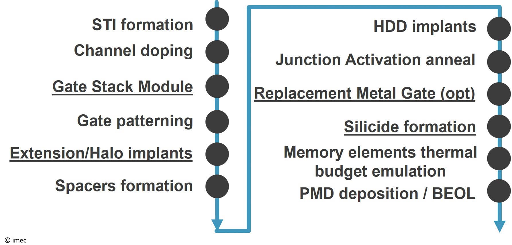
In addition to these specific requirements, there are a number of constraints that apply to all peripheral transistors. One critical issue is the thermal stability. In current DRAM process flows with DRAM memory arrays sitting next to the periphery, peripheral transistors are fabricated before DRAM memory elements. The periphery is thus subjected to several thermal treatments imposed by the fabrication of the storage capacitor, access transistor, and memory back-end-of-line. Peripheral transistors must, therefore, be able to withstand ‘DRAM memory anneal’ temperatures as high as 550-600°C for several hours. Next, the cost-effectiveness of DRAM chips must be preserved, driving the integration choices towards simpler process solutions than what logic flows are generally using. To keep costs down, the memory industry also favors a single technology platform for the various peripheral transistors – despite their individual needs. Additionally, there is a more aggressive requirement for low leakage and low power consumption, which benefits multiple DRAM use cases – especially mobile ones.
The combination of all these specifications makes a direct copy of the standard logic process flows impossible. It requires optimization of specific modules, including the transistors’ gate stack, source/drain junctions and source/drain metal contacts.
State-of-the-art DRAM periphery: from SiON-based gate stacks to high-k/metal gates
Until 2018 [3], DRAM peripheral transistors were predominantly made in planar logic MOSFET technology with poly-Si/SiO2 or poly-Si/SiON gates. These technologies were less advanced than the transistors used for high-performance logic in order to maintain the DRAM cost-per-bit trendline. However, an improved technology for the periphery became necessary to keep pace with the performance enhancement enabled by subsequent generations of DRAM memory. The most obvious candidate was moving to a planar transistor architecture with a high-k/metal-gate stack – a transition that occurred as early as 2007 in the high-volume manufacturing of logic technologies.
Since about 2007, imec, together with its partners, has actively explored a DRAM-compatible version of high-k/metal-gate transistors and proposed multiple material and integration options to the memory industry. Today, almost every device with a DRAM memory inside contains a planar peripheral transistor technology with high-k/metal gates, which imec has been pioneering for more than 15 years. Below is a grasp of some of the proposed material, module, and integration options, all differing in fabrication complexity and performance levels [1,2].
High-k/metal-gate integration: thermally stable gate-first and gate-last integration flows
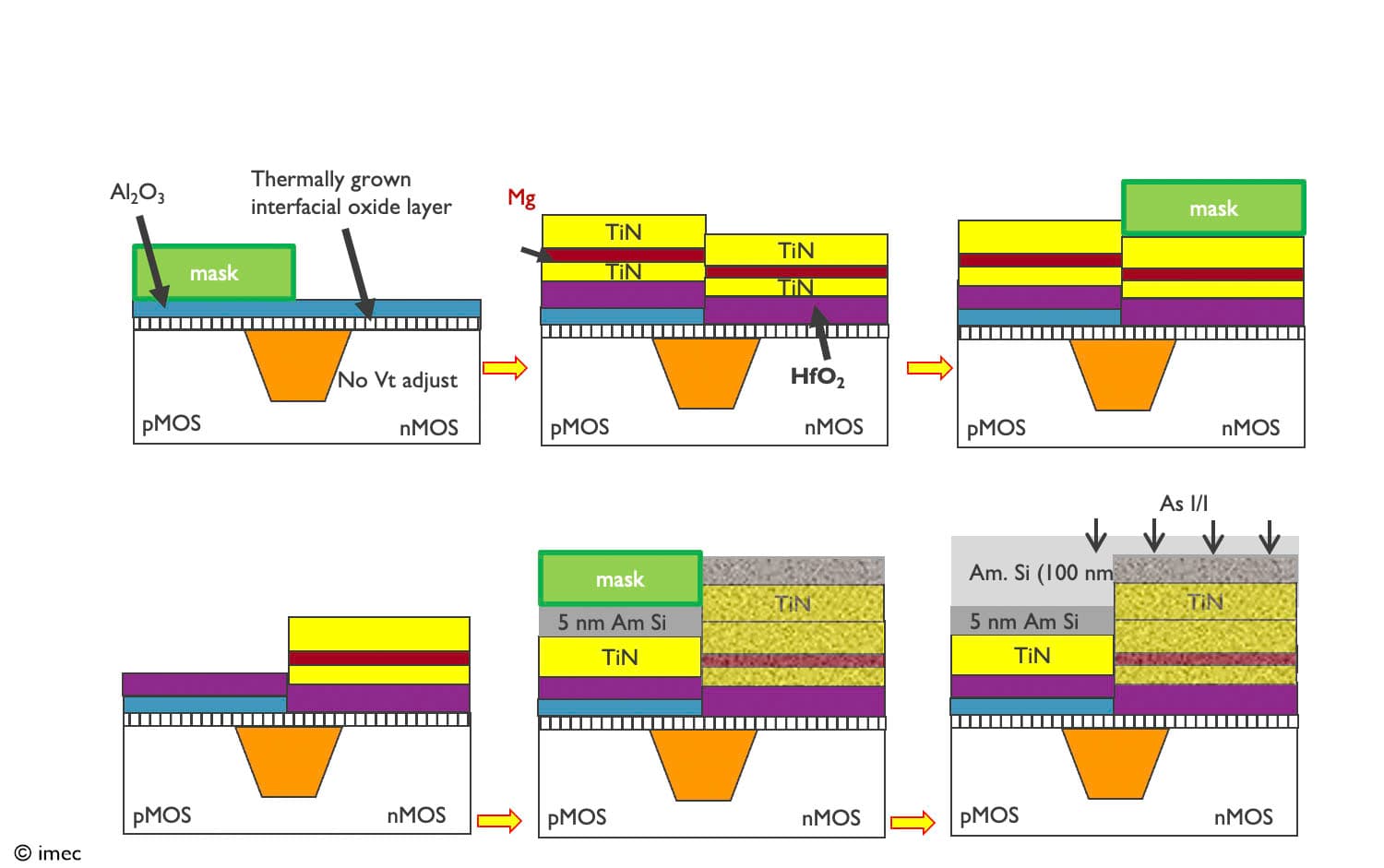
One of the solutions demonstrated by imec for potential early introduction was based on a gate-first integration approach, in which the metal gate is deposited before the high-temperature source/drain junction activation anneal. Gate stacks for nMOS and pMOS can be optimized separately by using different work function metals and layer thicknesses for the high-k/metal-gate stack (e.g., TiN/Mg/TiN for n; TiN for p).
One of the critical parameters is obtaining an effective work function that is low enough for nMOS and high enough for pMOS to ensure a good Ion/Ioff ratio. Researchers achieved this by doping the gate stacks (with different dopants for p- and nMOS), which enabled a shift in the threshold voltages. The choice of the dopant materials and their integration also provided a knob for improving the thermal stability of the gate stack and enabling the different Vth required by the DRAM chip. The DRAM-specific requirement for low gate leakage was addressed, among others, by adopting thicker gate stacks compared to logic-oriented solutions.
Imec also successfully demonstrated a thermally improved version of a gate-last integration approach, also called replacement metal gate (RMG) flow. In a gate-last flow, a poly-Si capped dummy gate is deposited and remains in place until the junction activation anneal is applied. After that, the dummy poly is replaced by the target metal gate.
Optimized source/drain junctions
Source/drain junctions are critical to ensure the functionality of MOSFET transistors. They are formed by creating a dopant gradient in the source/drain areas.As conduction channel lengths continued to shrink, ultra-shallow junctions became indispensable to ensure good electrostatic control over the channel. However, for peripheral transistors, the thermal treatments during DRAM memory anneal trigger an unwanted diffusion of the dopants, requiring more complex process flows to maintain the dopant gradient. This issue can be addressed by changing the junction implant scheme using, e.g., pre-amorphization implants and junction co-implants. Imec demonstrated several sets of optimized junctions, suited for various threshold voltage targets.
A thermally stable silicide process
A general challenge for all transistors is to keep the source/drain contact resistance as low as possible. Source/drain contacts are formed by bringing a metal in contact with the source/drain regions, creating a Schottky barrier at the interface. To ensure low resistance, two techniques are typically applied: (1) heavy doping of the source/drain regions and (2) complete silicidation of the source/drain areas – the silicides being formed through the reaction of the contact metal with the doped Si. Ni(Pt) silicide, traditionally used in logic devices, cannot, however, withstand the DRAM-related anneal temperatures. Imec proposed a thermally stable NiPt-based silicide module with low contact resistance, by implementing additional implants and annealing steps for silicide stabilization.
The next generation: a thermally stable FinFET-based peripheral platform for improved power, performance, and area
Applications like automotive, AI and machine learning impose increasingly stringent requirements on DRAM memories, driving the need for faster, more reliable and power efficient peripheral transistors. One option is to re-trace the path of ‘logic’ and move from planar high-k/metal-gate transistors to FinFETs. The logic roadmap made this transition as early as 2011 after R&D clearly showed the superior performance of transistors with fin-shaped conduction channels: improved Ion/Ioff, better short channel control, higher drive current at reduced footprint (due to a higher effective width of the channel), and lower power consumption – while keeping cost under control. On top of that, the use of tall fins provides a way to reduce the threshold voltage mismatch, which can particularly benefit the DRAM sense amplifiers.
Just like for the planar versions, the DRAM-specific requirements preclude a copy-paste of FinFET process flows developed for regular logic. In response, imec developed a thermally stable FinFET-based peripheral technology platform with integrated modules optimized for DRAM. Multiple flavors with different performance-cost trade-offs have been proposed to the industry for their next-generation DRAM products.
Thermally stable gate-first and gate-last FinFET integration flows
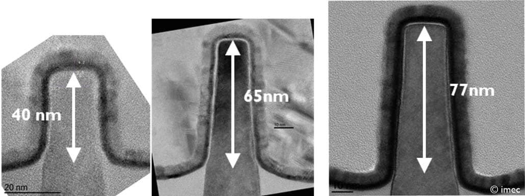
In 2021, imec reported the first experimental demonstration of a thermally robust integration flow for FinFETs using an optimized gate-first approach for implementing the high-k/metal-gate stack. Compared to a traditional gate-first approach, the modified flow implements gate stacks with the same thickness and the same work function metal for both n- and pMOS. So-called Vth shifter materials are then diffused into the high-k dielectric to tune the effective work function of the n- and pMOS devices. This modified gate-first approach reduces the gate asymmetry and enhances the thermal stability of the flow. By using this flow, the researchers demonstrated improved Ion/Ioff and short channel control over planar high-k/metal-gate counterparts. These metrics did not degrade after the DRAM-specific anneal. Flavors with taller fins (up to 80nm height) have also been developed, with improved threshold voltage mismatch and area gain [4,5].
A drawback of the gate-first integration approach is the relatively high threshold voltage, which originates from the impact of the high-temperature anneal on the gate stack during junction activation. This issue can be solved using a gate-last (or RMG) integration approach, which, however, comes with additional process steps. At IEDM in 2022, imec showed a thermally stable version of a FinFET gate-last flow [6].
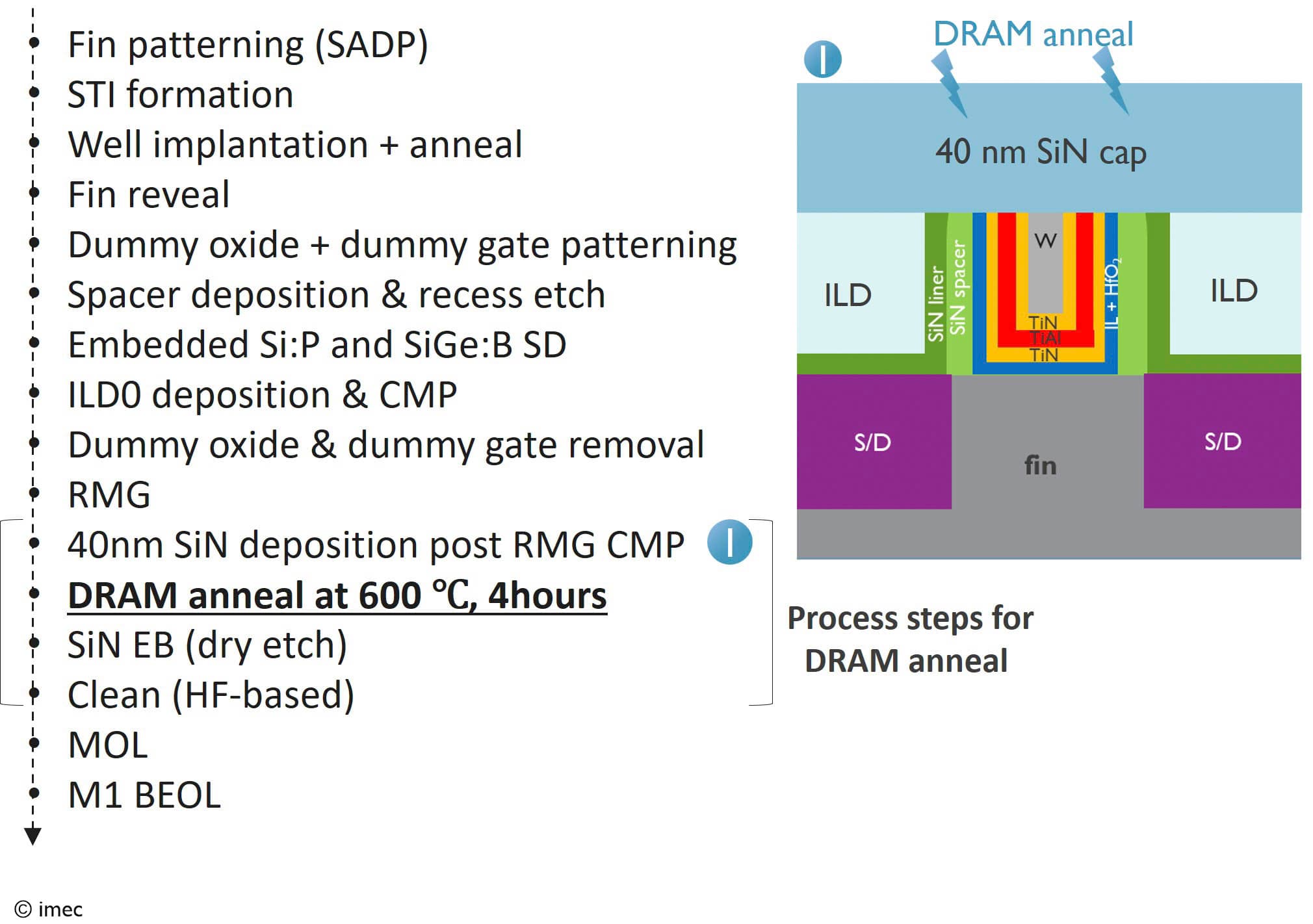
An optimized thermally stable gate-last FinFET flow, with a Mo-based work function metal for pMOS
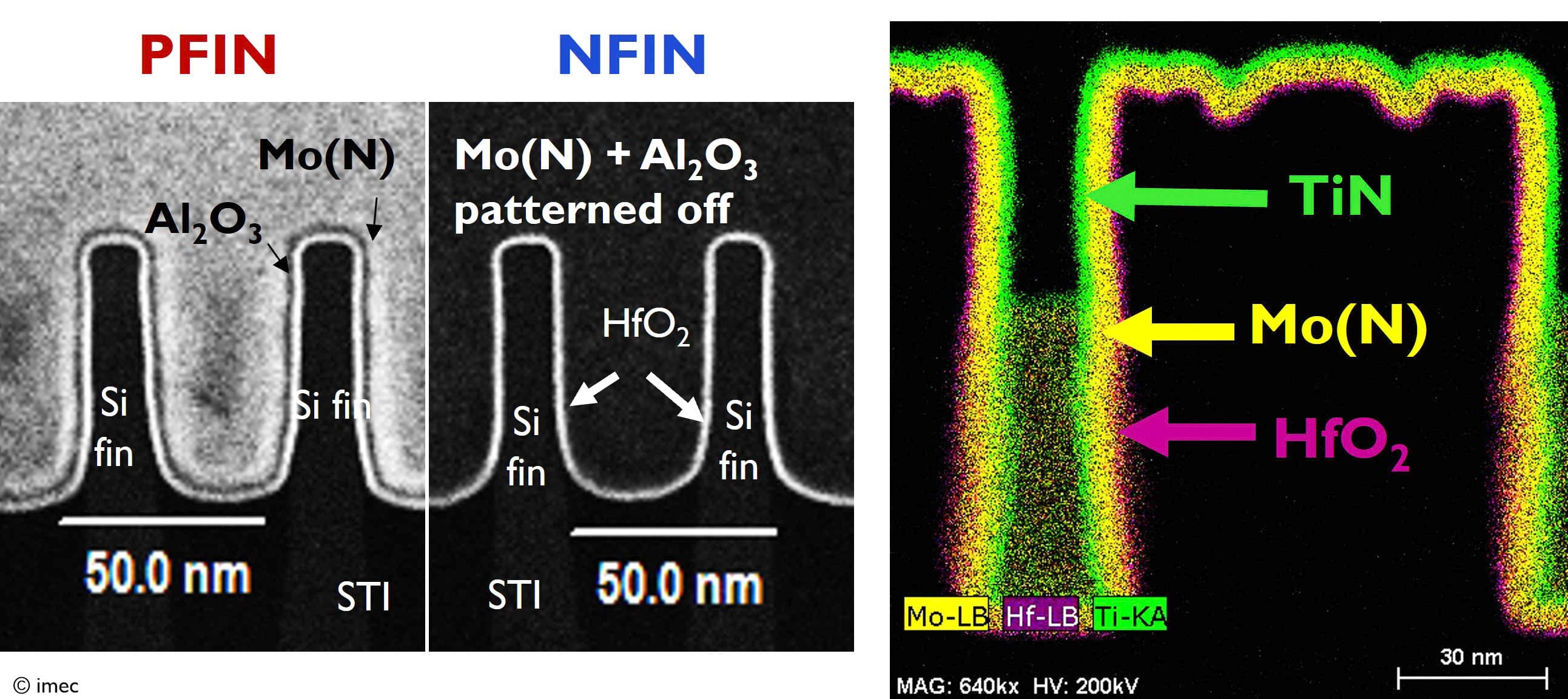
Typical for a gate-last flow is the use of different work function metals for nMOS and pMOS devices. At VLSI in 2024, imec demonstrated the performance benefits of using a novel Mo-based work function metal for pMOS instead of the conventional TiN-based approach. The new gate stack module was successfully integrated into a gate-last FinFET flow and proven to be thermally stable. The DRAM-compatible flow with integrated Mo-based p-work function metal yielded sufficiently low Ioff current and low threshold voltage (0.12V) for the pMOS devices. The FinFETs were also benchmarked against a thermally stable planar high-k/metal-gate reference, showing a three times higher Ion (at target Ioff) for the same Si footprint. These results make the thermally stable gate-last FinFET flow a valuable candidate for sub-10nm DRAM peripheral logic [7].
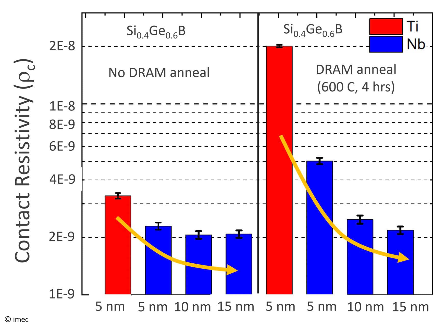
Thermally stable Nb-based metal contacts with low contact resistance
In earlier work on planar high-k/metal-gate based peripheral transistors, imec researchers lowered the source/drain contact resistance by improving the dopant profile and adding pre-amorphization implants. At IEDM in 2024, imec introduced a different approach: replacing the conventional Ti contact metal with Nb for pMOS devices. The thermal stability of the Nb-based contact module was demonstrated for the first time. In addition, superior performance was observed when integrated into the gate-last FinFET platform: record low contact resistance, reduced overall parasitic resistance and improved Ion [8].
Outlook
Imec pioneered peripheral transistor technology ten years ahead of the industry’s mass production introduction. In their most recent R&D work, imec demonstrated an industry-relevant, thermally stable FinFET-based platform to meet the requirements for sub-10nm DRAM.Multiple flavors have been developed as possible solutions for next-generation DRAM products, providing different levels of fabrication complexity and transistor performance.
More disruptive concepts are envisioned in the longer term to continue the DRAM scaling path. One of these is building the periphery on a separate wafer and integrating it with the memory array using advanced wafer bonding techniques. Although this approach comes with additional process steps, a true benefit is the relaxed requirement for thermal stability, as the periphery is now manufactured separately from the memory array. Imec recently initiated R&D work on peripheral transistors for this new DRAM architecture, guided by insights obtained from planar and FinFET-based technology.
This article was originally published in EDN (part 1 and part 2).
References
[1] ‘1T-1C dynamic random access memory status, challenges and prospects’, A. Spessot et al., IEEE transactions on electron devices, Vol. 67, n°4 (2020);
[2] ‘Optimized material solutions for advanced DRAM peripheral transistors’, A. Spessot et al., Phys. Status Solidi A, 1–10 (2016) / DOI 10.1002/pssa.201532791;
[3] Samsung develops industry’s first HKMG-Based DDR5 memory; ideal for bandwidth-intensive advanced computing applications, Samsung Newsroom
[4] ‘80nm tall thermally stable cost effective FinFETs for advanced dynamic random access memory periphery devices for artificial intelligence/machine learning and automotive applications’, A. Spessot et al., 2021 Jpn. J. Appl. Phys. 60 SBBB06;
[5] ‘High performance thermally resistant DRAM peripheral CMOS FinFETs with Vth tunability for future memories’, R. Ritzenthaler et al., VLSI-T 2022, 306-307;
[6] ‘FinFETs with thermally stable RMG gate stack for future DRAM peripheral circuits’, E. Capogreco et al., IEDM 2022, DOI: 10.1109/IEDM45625.2022.10019422;
[7] ‘DRAM-peri FinFET – a thermally-stable high-performance advanced CMOS RMG platform with Mo-based pWFM for sub-10nm DRAM’, J. Ganguly et al., VLSI 2024;
[8] ‘Nb contacts for thermally-stable high-performance logic and memory peripheral transistor’, R. Sarkar et al., IEDM 2024.
Authors

Alessio Spessot
Alessio Spessot received an M.Sc. degree in Physics (magna cum laude) from Trieste University in 2003 and a Ph.D. degree in Solid-State Physics from the Modena University in 2006. He has worked for STMicroelectronics, Numonyx, and Micron. He has been involved in developing advanced CMOS, DRAM, NAND, emerging memory array, and periphery. Since 2016, he has been with imec, where he is currently Technical Account Director.

Naoto Horiguchi
Naoto Horiguchi is a director of the logic CMOS scaling program in imec, Leuven, Belgium. He started his carrier in semiconductor device R&D in Fujitsu Laboratories Ltd. in 1992. In 1992-1999, he was engaged in device development by using semiconductor nanostructures in Fujitsu laboratories Ltd. and University of California, Santa Barbara. In 2000 to 2006, he was engaged in 90-45nm CMOS technology development in Fujitsu Ltd. as a lead integration engineer. From 2006, he is with imec, Leuven, Belgium, where he is engaged in advanced CMOS device R&D together with worldwide industrial partners, universities and research institutes. His current focus is CMOS device scaling down to 2nm technology node and beyond.
Discover more

Imec achieves breakthroughs in ferroelectric memory research for next-generation memory solutions to meet AI-era data needs
Read more
Sony and imec unveil high-density backside connectivity module enabling next-generation 3D chip integration
Read more
ASML, TSMC and imec bring industry-ready 2D-material transistors closer with breakthrough 300mm integration
Read more