Naoto Horiguchi
Naoto Horiguchi is a director of the logic CMOS scaling program in imec, Leuven, Belgium. He started his carrier in semiconductor device R&D in Fujitsu Laboratories Ltd. in 1992. In 1992-1999, he was engaged in device development by using semiconductor nanostructures in Fujitsu laboratories Ltd. and University of California, Santa Barbara. In 2000 to 2006, he was engaged in 90-45nm CMOS technology development in Fujitsu Ltd. as a lead integration engineer. From 2006, he is with imec, Leuven, Belgium, where he is engaged in advanced CMOS device R&D together with worldwide industrial partners, universities and research institutes. His current focus is CMOS device scaling down to 2nm technology node and beyond.
Authored articles
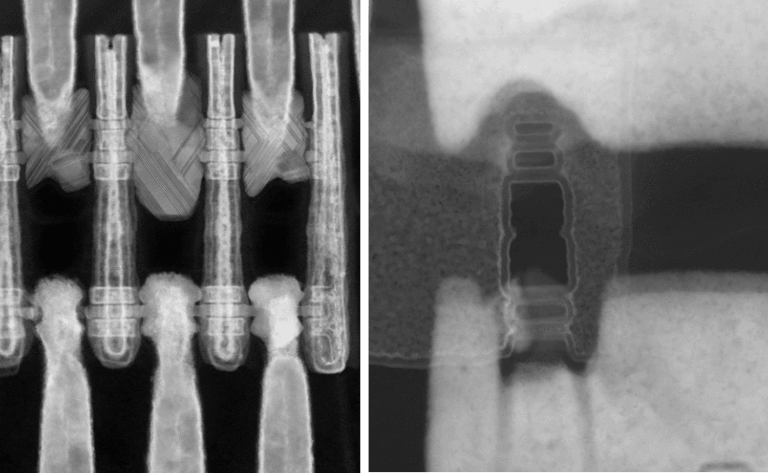
Performance boosters to scale monolithic CFET across multiple logic technology nodes
DTCO study supported by experimental demonstration of hybrid channel orientations which are needed for A3
Read more
A technology platform for thermally stable DRAM peripheral transistors
Imec proposes different material and integration options in response to the evolving needs of the DRAM periphery
Read more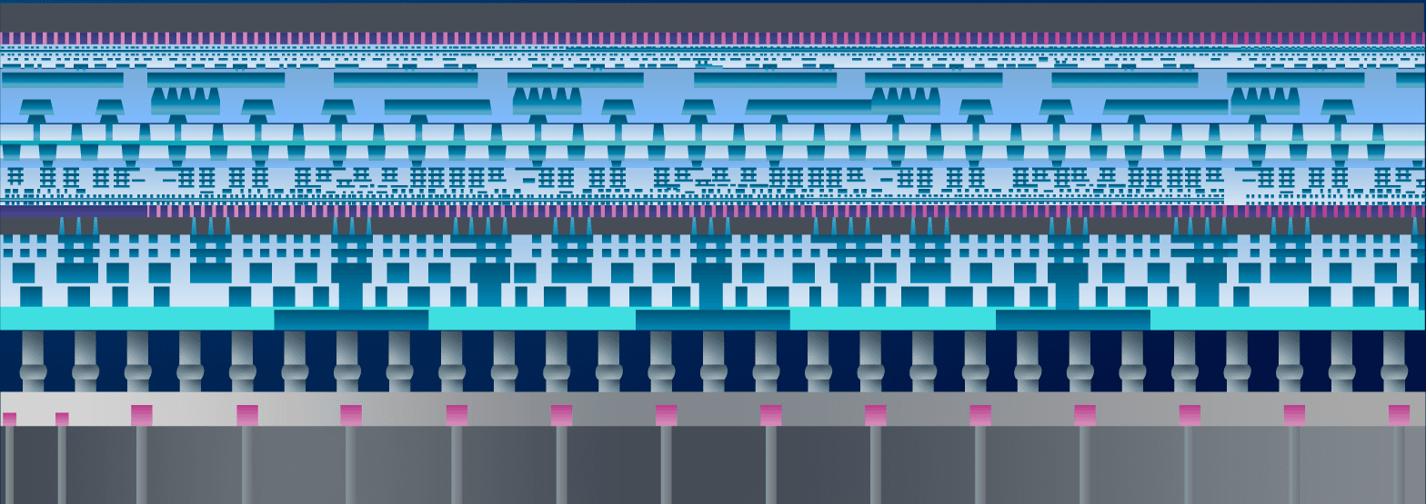
Backside power delivery
How to power chips from the backside: benefits and building blocks of a backside power delivery network.
Read more
Imec puts complementary FET (CFET) on the logic technology roadmap
Improved process flows make sequential CFET an attractive alternative to monolithic CFET.
Read more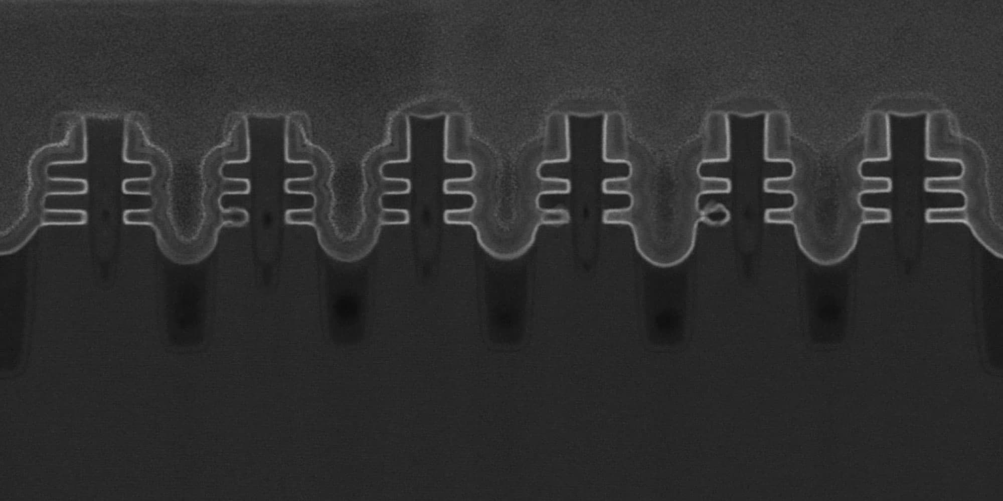
Entering the nanosheet transistor era
Reviewing benefits and challenges of nanosheet device architectures for 3nm and beyond: nanosheet, forksheet and CFET
Read more
Logic technology scaling options for 2nm and beyond
A roadmap marked by increased synergy between advanced logic device and nano-interconnect research
Read more
Imec demonstrates critical building blocks for a backside power delivery network
In several papers presented at the 2021 Symposia on VLSI Technology and Circuits (VLSI 2021), imec reports progress in developing enabling technologies for a backside power delivery network. First, the impact of backside wafer processing on the performance of ‘frontside’ FinFET devices was investigated. Second, the team revealed new approaches for efficient power delivery and conversion that are compatible with backside processing. And finally, the impact of backside connection on I/O performance is discussed from a system-technology co-optimization (STCO) perspective.
Read more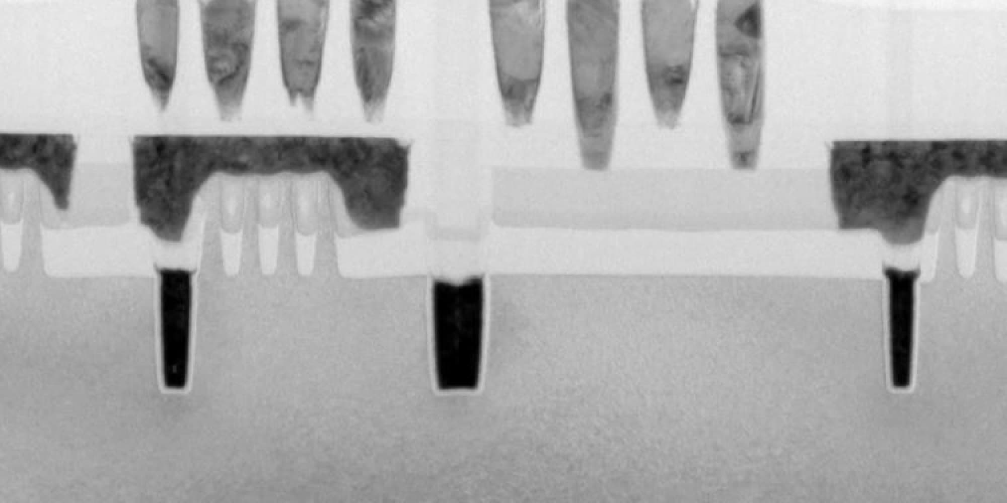
A view on the logic technology roadmap
Advancing the front-end, back-end and middle-of-line towards the 1nm technology generation
Read more