Imec demonstrates critical building blocks for a backside power delivery network
In several papers presented at the 2021 Symposia on VLSI Technology and Circuits (VLSI 2021), imec reports progress in developing enabling technologies for a backside power delivery network.
First, the impact of backside wafer processing on the performance of ‘frontside’ FinFET devices was investigated.
Second, the team revealed new approaches for efficient power delivery and conversion that are compatible with backside processing.
And finally, the impact of backside connection on I/O performance is discussed from a system-technology co-optimization (STCO) perspective.

Backside power delivery: promises and challenges
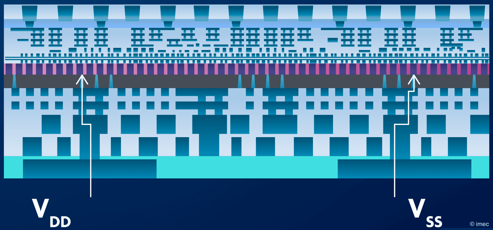
The goal of a power delivery network is to provide power and reference voltage to the active devices on the die, in the most efficient way. This network is essentially a network of interconnects that is separate from the signal network. Traditionally, both networks are fabricated through back-end-of-line (BEOL) processing on the frontside of the wafer. But we can also envision to move the power distribution to the backside of the silicon wafer, which today serves only as a carrier. This would allow direct power delivery to the standard cells, and promises to enhance system performance, increase chip area utilization, and reduce BEOL complexity.
Arm, in collaboration with imec, earlier showed the beneficial impact of using backside power delivery as a scaling booster in the design of a central processing unit (CPU). Using backside power delivery turned out to be the most efficient way of delivering power to the circuits. For example, it largely improves the supply-voltage (or IR) drop that is caused by a resistance increase in the BEOL of traditional designs. In the ‘winning’ processor design, the backside power delivery is connected to a buried power rail (BPR), a structural scaling booster in the form of a local power rail that is buried in the chip’s front-end-of-line. [1,2]
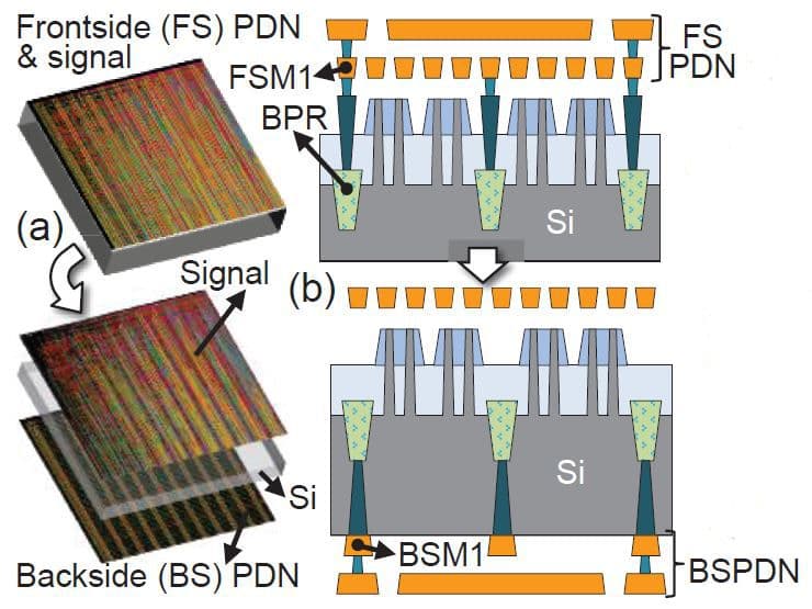
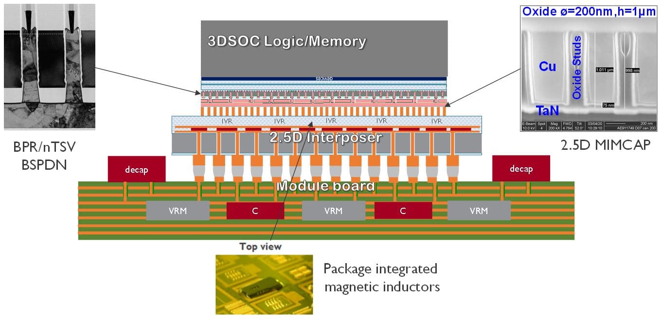
The realization of true backside power delivery networks comes however with additional technological complexities. A dedicated wafer thinning process is needed in combination with the ability to process nano-through-silicon-vias (n-TSVs) that electrically connect the backside to the frontside of the device wafer. In addition, several questions need to be answered. Will this backside wafer processing impact the active devices that are already present in the wafer’s frontside? And if we deliver power through the backside, how can this be done in the most efficient way? Can we implement efficient voltage regulation and power conversion techniques that are compatible with backside processing? And finally, how to bring input/output (I/O) circuits to the backside of the wafer?
In five papers presented at the 2021 VLSI Symposium, imec shows progress in developing the critical technology building blocks needed for realizing backside power delivery networks as a structural scaling booster to further the path of Moore’s Law. Besides, the authors show that the wafer’s backside can create a very dynamic design space with new design options to optimize the power delivery for scaled systems.
First characterization of backside connected FinFETs
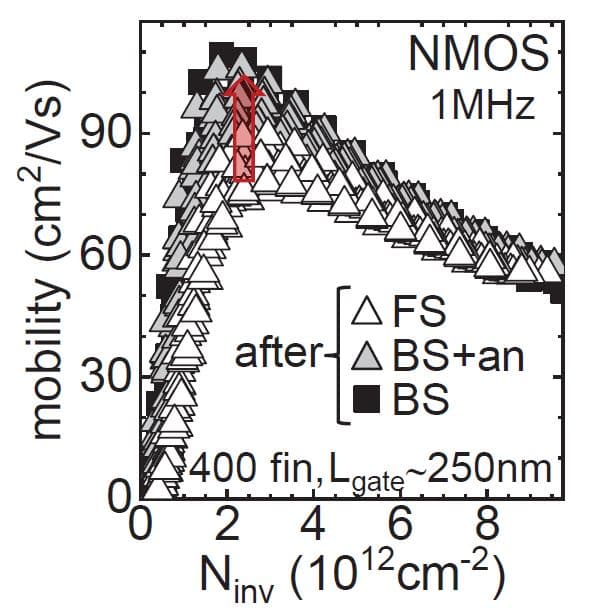
For the first time, imec has evaluated the impact of backside wafer thinning and n-TSV fabrication on the characteristics of scaled Si-channel FinFET test devices (gate length ≥20nm), built in the wafer’s frontside. The backside connectivity was realized through tungsten-filled n-TSVs that land on metal-1 pads in the wafer’s frontside. Naoto Horiguchi, director CMOS device technology at imec: “The most important conclusion of this work is that wafer thinning and n-TSV processing in the backside did not show any negative impact on the performance of the FinFETs, except for a slight degradation of the pMOS drive current. For nMOS, an even higher mobility and drivability (up to 15%) were found after backside processing, and no bias temperature instability (BTI) degradation was observed. In this work, wafers were thinned down to final Si thicknesses ranging between 20 and 370nm.” More details are included in the 2021 VLSI paper by A. Veloso et al. [VLSI-1]
Progress in wafer-thinning and n-TSV processing
Wafer thinning and via-last n-TSV fabrication processes used in this study are being developed and optimized in the frame of imec’s 3D integration program. Eric Beyne, senior fellow, VP R&D and program director 3D system integration program at imec: “First, an epitaxial stack of Si/SiGe layers is grown on top of a bulk Si substrate. The SiGe layer later serves as an etch stop layer for ending the wafer thinning. The frontside, including the FinFET devices, is then built on top of this Si ‘capping’ layer. Cu metal-1 metallization completes the frontside processing. Next, the wafer is flipped over, and the ‘active’ frontside of the wafer is bonded to a second ‘carrier’ Si wafer using a low-temperature wafer-to-wafer bonding technique. The backside of the first wafer can now be thinned down to where the SiGe etch stop layer is located. Thinning down to a few 100nm is required to expose the high-aspect ratio nano-meter scale TSVs. After SiGe removal, the process is completed by n-TSV patterning and tungsten fill, and backside metallization.”
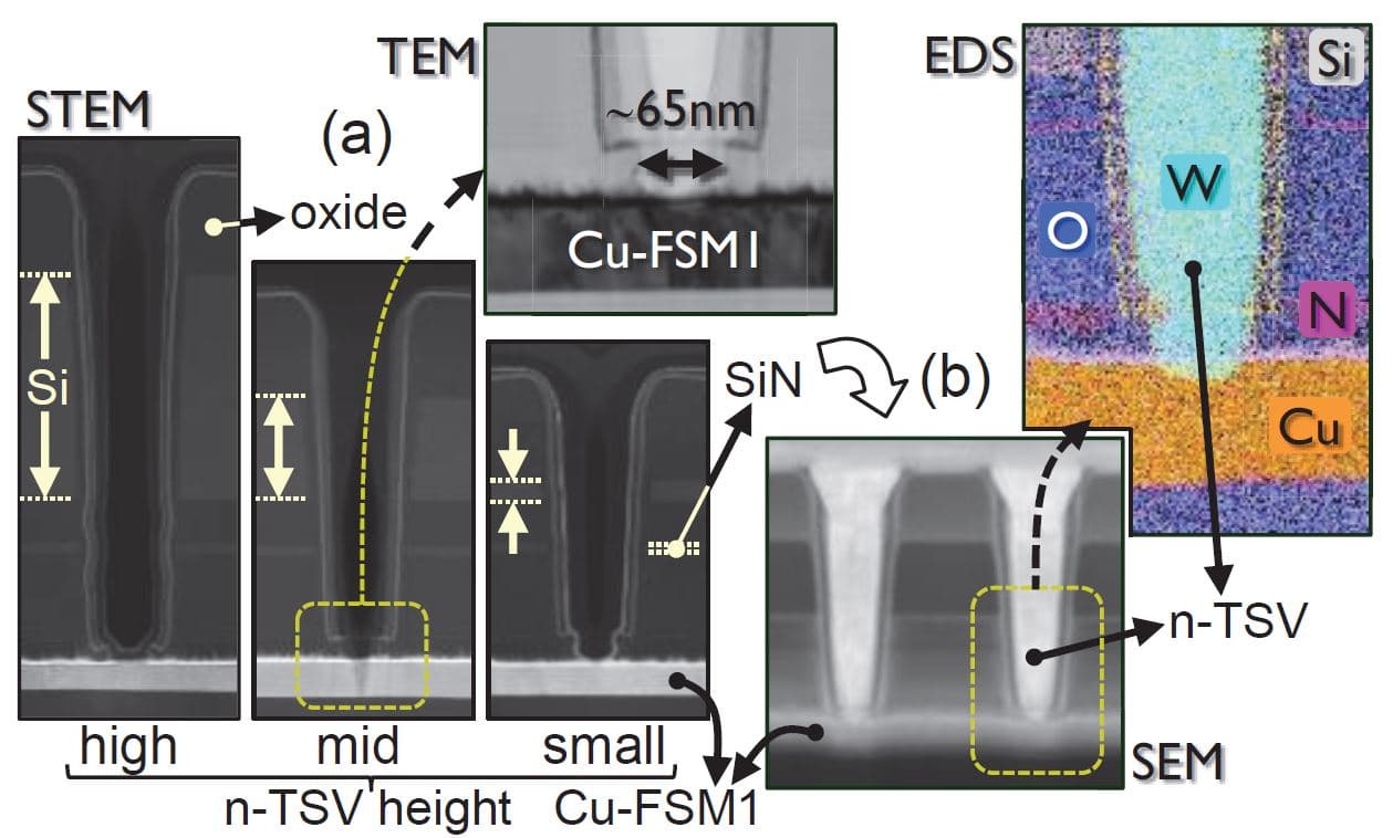
In the above approach for backside power delivery, n-TSVs electrically connect the backside metal-1 to the frontside metal-1. Their electrical performance was successfully verified in specific n-TSV configurations (such as daisy chains). The n-TSVs can alternatively land on buried power rails implemented in the wafer’s frontside. Process steps for this challenging configuration are under development.
MIMCAPs, voltage regulators and power converters for increased power delivery efficiency
Imec looks into new methodologies to realize effective power delivery networks from the broader perspective of scaled systems – combining on-chip as well as off-chip components. This is one of the topics that is being discussed in the invited VLSI paper by Geert Van der Plas and Eric Beyne [VLSI-2]. “In general, the power supply in advanced IC systems is seriously challenged by increased power density, lower supply voltage (and hence, larger currents), aggressive IR drop, voltage noise and electromigration,” says Geert Van der Plas, program manager at imec. “Removing the power delivery as well as the power conversion from the logic die’s frontside to its backside can boost the system performance by specific designs. An example is a metal-insulator-metal capacitor (or MIMCAP) that serves as a decoupling capacitor – a component that allows to stabilize the voltage supply by de-coupling the noise generated by the transistors switching activity. We have shown that integrating this passive MIMCAP component in the wafer’s backside can reduce the supply ‘bounce’ with a factor of 15.”
In another VLSI paper by H. Lin et al, it is demonstrated how such an integrated MIMCAP can also be part of a charge pump that serves as a down-conversion integrated voltage regulator with 91.5% efficiency [VLSI-3]. A related paper by the same author discusses an implementation of a power converter for backside power delivery. The converter consists of a laterally diffused power MOS (LDMOS) that is implemented in the logic die’s backside, in combination with an off-chip, package-integrated transformer with an innovative magnetic material. This approach essentially allows us to lower the voltage from ~12V to ~1V (at transistor level) inside the package, avoiding large currents to flow through the solder balls [VLSI-4].
Tackling the I/O challenge for backside power delivery networks
Delivering power through the backside will eventually also affect the I/O implementation, which should now also be moved to the backside. Compared to conventional frontside I/O cells, additional capacitances coming from the backside power delivery network might impact the I/O interfaces. The VLSI paper by W.-C. Chen et al. deals with the I/O development roadmap from a system-technology co-optimization (STCO) perspective. As part of the paper, the impact of the fully back-side connection (with buried power rail) on I/O performance is investigated, and layout options (such as deep trench isolation) to reduce the extra capacity are discussed. [VLSI-5]
Want to know more?
- [1] ‘Arm shows backside power delivery as path to further Moore’s Law’, IEEE Spectrum
- [2] ‘Imec demonstrates excellent performance of Si FinFET CMOS devices with integrated tungsten buried power rail’, imec press release
- Interested in receiving any of the VLSI 2021 papers below? Fill in our contact form.
- [VLSI-1] ‘Enabling logic with backside connectivity via n-TSVs and its potential as a scaling booster’, A. Veloso et al., VLSI 2021
- [VLSI-2] ‘Design and technology solutions for 3D integrated high performance systems’, Geert Van der Plas and Eric Beyne, VLSI 2021, invited
- [VLSI-3] ‘91.5%-efficiency fully integrated voltage regulator with 86fF/μm2-high-density 2.5D MIM capacitor’, H. Lin et al., VLSI 2021
- [VLSI-4] ‘Backside power delivery with a direct 14:1/19:1 high-ratio point-of-load power converter for servers and datacenters’, H. Lin et al., VLSI 2021
- [VLSI-5] ‘External I/O interfaces in sub-5nm GAA NS technology and STCO scaling options’, W.-C. Chen et al, VLSI 2021
- Want to know more about imec's presence at 2021 VLSI? Check out our program.
Authors

Naoto Horiguchi
Naoto Horiguchi is a director of the logic CMOS scaling program in imec, Leuven, Belgium. He started his carrier in semiconductor device R&D in Fujitsu Laboratories Ltd. in 1992. In 1992-1999, he was engaged in device development by using semiconductor nanostructures in Fujitsu laboratories Ltd. and University of California, Santa Barbara. In 2000 to 2006, he was engaged in 90-45nm CMOS technology development in Fujitsu Ltd. as a lead integration engineer. From 2006, he is with imec, Leuven, Belgium, where he is engaged in advanced CMOS device R&D together with worldwide industrial partners, universities and research institutes. His current focus is CMOS device scaling down to 2nm technology node and beyond.

Geert Van der Plas
Geert Van der Plas obtained a Ph.D. degree in Applied Sciences from the Katholieke Universiteit Leuven, Belgium, in 2001. He joined imec, Belgium, in 2003. He has been working on energy efficient data converter, power/signal integrity and 3D integration technologies. Currently he is program director of the XTCO Power program addressing system scaling challenges related to power delivery for high performance, energy efficient systems. In the Cross-technology co-optimization (XTCO) program, STCO/DTCO methodology is applied to align technology roadmaps with application needs. Geert’s interests are in system exploration and optimization, modeling and design enablement.

Eric Beyne
Eric Beyne obtained a degree in electrical engineering in 1983 and the Ph.D. in applied sciences in 1990, both from the Katholieke Universiteit Leuven, Belgium. Since 1986 he has been with imec in Leuven, Belgium where he has worked on advanced packaging and interconnect technologies. Currently, he is imec fellow and program director of imec’s 3D system integration program. He received the European Semi Award 2016 for contributions to the development of 3D technologies.
Discover more

Imec highlights benefits of 3D-SOC design and backside interconnects for future high-performance systems
Read more
Imec and EV Group demonstrate wafer-to-wafer hybrid bonding with 200nm interconnect pitch and record high overlay accuracy
Read more