Eric Beyne
Eric Beyne obtained a degree in electrical engineering in 1983 and the Ph.D. in applied sciences in 1990, both from the Katholieke Universiteit Leuven, Belgium. Since 1986 he has been with imec in Leuven, Belgium where he has worked on advanced packaging and interconnect technologies. Currently, he is imec fellow and program director of imec’s 3D system integration program. He received the European Semi Award 2016 for contributions to the development of 3D technologies.

Authored articles
A path to high-density front- and backside wafer connectivity
Advances in wafer-to-wafer hybrid bonding and backside technologies take CMOS 2.0 from concept to reality, offering more options for compute system scaling
Read more
Chiplets: Piecing Together the Next Generation of Chips (Part II)
Testing the limits: standardization and optimization of chiplet test protocols
Read moreChiplets: Piecing Together the Next Generation of Chips (Part I)
Bridging the gap: innovations in chiplet interconnect technology
Read more
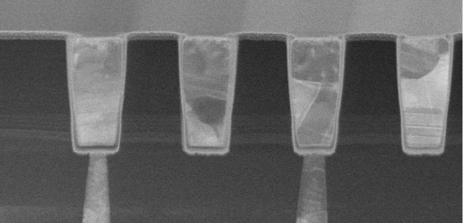
Wafer-to-wafer hybrid bonding: pushing the boundaries to 400nm interconnect pitch
Innovations in Cu/SiCN bonding technology are driven by memory-on-logic stacking needs
Read more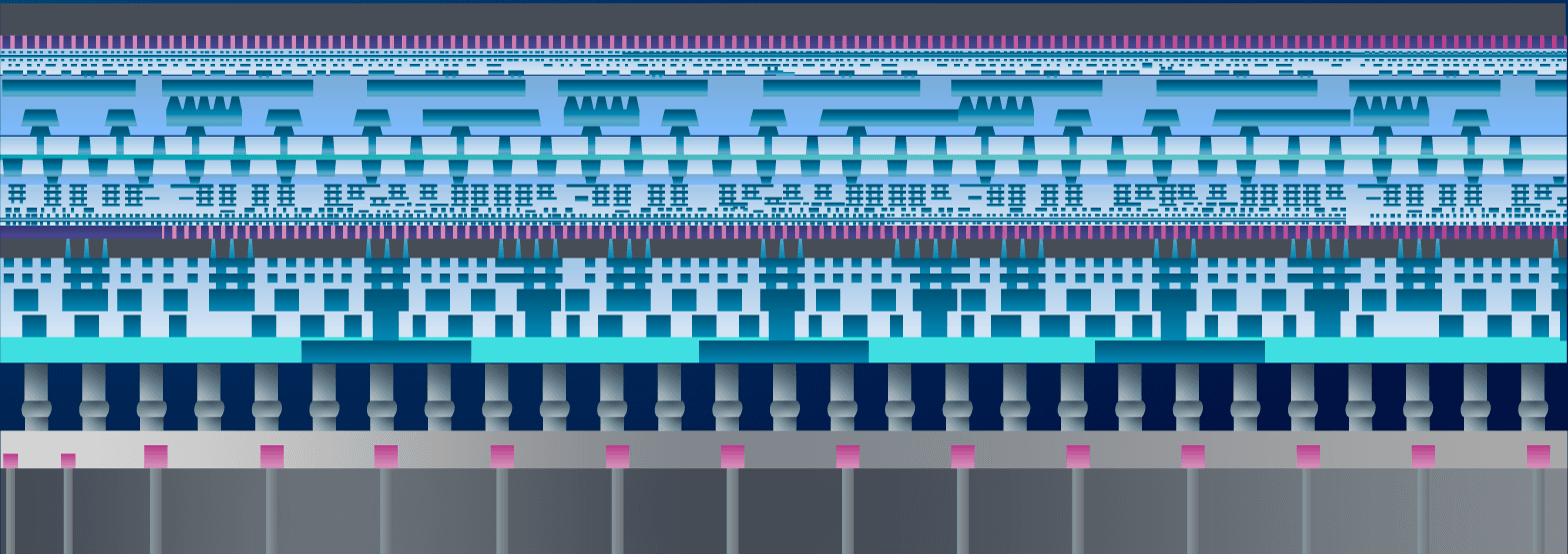
Backside power delivery
How to power chips from the backside: benefits and building blocks of a backside power delivery network.
Read more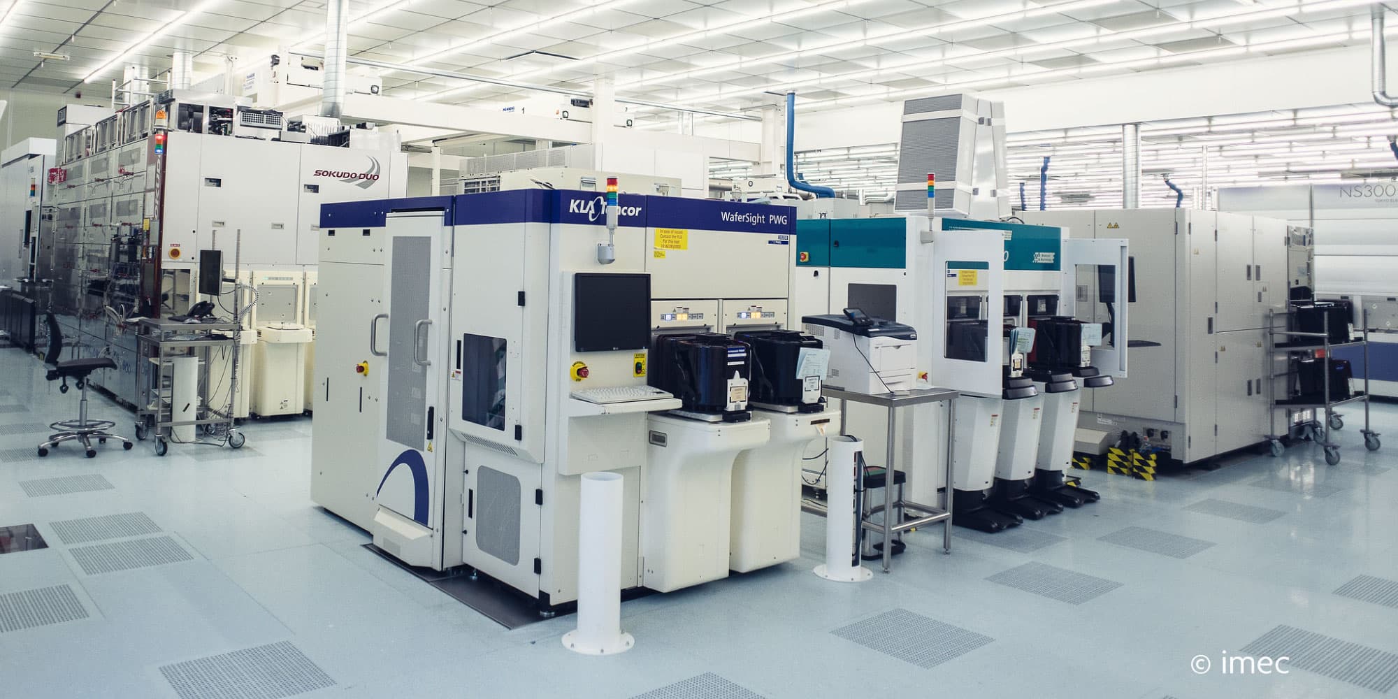
Imec highlights benefits of 3D-SOC design and backside interconnects for future high-performance systems
3D system-on-chip (3D SOC), enabled by electronic design automation (EDA) and 3D process technologies, is an attractive heterogeneous integration approach for addressing the memory wall in high-performance systems. Further performance gains at the system level can be achieved when the backside of one of the integrated wafers is exploited for either power delivery, signal routing or both. In this article, Dragomir Milojevic, Geert Van der Plas and Eric Beyne shed light on these promising approaches. The benefits of 3D-SOC design and of backside interconnects in specific circuits are highlighted in two papers presented at the 2021 IEEE International Electron Devices Meeting (IEDM).
Read more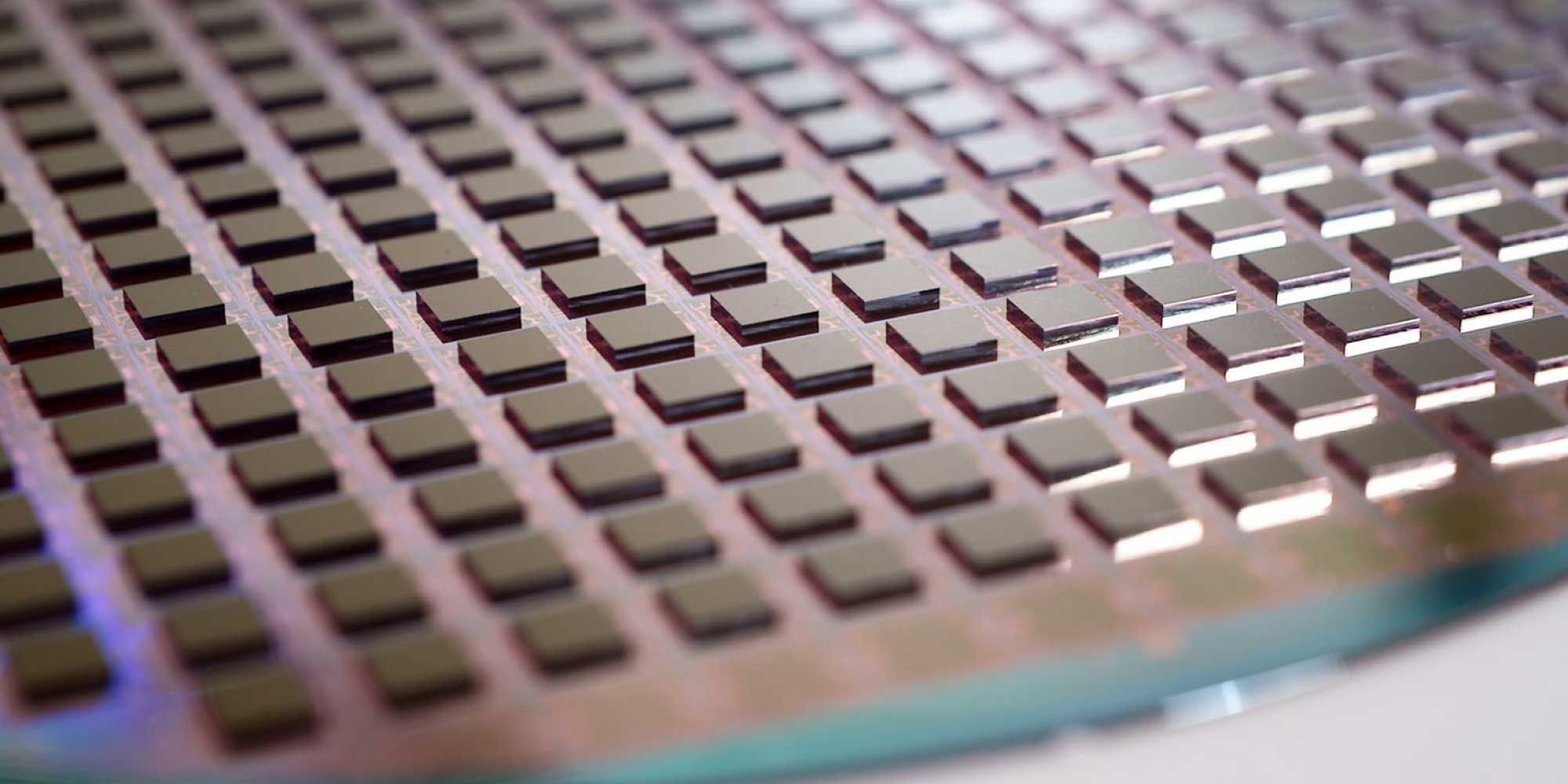

Imec demonstrates critical building blocks for a backside power delivery network
In several papers presented at the 2021 Symposia on VLSI Technology and Circuits (VLSI 2021), imec reports progress in developing enabling technologies for a backside power delivery network. First, the impact of backside wafer processing on the performance of ‘frontside’ FinFET devices was investigated. Second, the team revealed new approaches for efficient power delivery and conversion that are compatible with backside processing. And finally, the impact of backside connection on I/O performance is discussed from a system-technology co-optimization (STCO) perspective.
Read more