A view on the 3D technology landscape
Design and technology options for 3D systems-on-chip
In short
In industry, we see more and more examples of systems being built through heterogeneous integration leveraging 2.5D or 3D connectivity.
In this interview, Eric Beyne, Senior Fellow, VP R&D and Program Director 3D System Integration at imec, reviews the trends and discusses the technologies that are needed for building the next-generation 3D systems-on-chip.
The progress reported at all levels will take system design and development into the next level, promising big rewards in the system’s power-performance-area-cost (PPAC) metrics.
Which main trends will mark your research domain in the coming years?
Eric Beyne: “Traditional CMOS technology scaling – resulting in monolithic CMOS single-chip systems-on-chip (SOCs) – will continue into the next decade through innovations in technology, materials and device architectures. CMOS scaling is increasingly being complemented by design-technology-co-optimization (DTCO) to improve the system’s power, performance, area and cost (PPAC). But with increasing cost and technology complexity, these approaches no longer deliver sufficient gains at the system level. This is especially true for data-intensive high-performance applications that are challenged by the so-called memory wall – the difficulty of accessing data quickly enough.
To further optimize the system’s PPAC metrics, the semiconductor industry is increasingly looking at multi-chip heterogeneous integration solutions.
Following this approach, the different functions on the chip can be optimized separately (using different (node) technologies), and shorter and faster connections can be realized between a system’s sub-components. First ‘heterogeneous’ implementations (such as high-bandwidth memories (HBMs)) mainly rely on 2.5 or 3D chiplet approaches involving separately designed and processed chiplet dies. Die-to-die communications are mainly realized using standardized interface physical layer (PHY) IP blocks, limiting the applications to latency-tolerant functions such as last-level memory caching.
Although the chiplet approach has significantly broadened the scope of heterogeneous system integration, we will witness an evolution towards true 3D-SOC designs where intermediate interface PHY layers are no longer needed. These 3D SOCs will be enabled by cleverly co-designing the different 3D partitions and by realizing direct die-to-die 3D interconnects.”
Which avenues is imec exploring to overcome the challenges ahead?
“Realizing optimal 3D SOCs calls for system architecture re-design, requiring innovations in electronic design automation (EDA) tools to enable the co-design of different devices in one view.
In that context, imec teams up with its partners in EDA software to develop solutions for automated netlist partitioning and 3D path optimization. In this context, we recently reported a new 3D design flow – developed in collaboration with Cadence. The software helps predicting whether the proposed 3D partitioning will result in robust and fully functioning 3D SOCs, bringing heterogeneous integration a step closer to industrial reality.
Other contributions come from 3D integration technology development – a key enabler for 3D SOCs. Together with our material and equipment suppliers, we develop a variety of 3D interconnect technologies spanning a broad range of interconnect pitches, from mm (package stacking) to less than 100nm (transistor stacking). And we develop efficient cooling solutions (such as impingement-based cooling) to more efficiently deal with the ever-increasing power that builds up in increasingly dense high-performance systems-on-chip.”
Any other technology developments that are worth mentioning?
“Backside power delivery (BSPD) is another promising technology development that can help realizing 3D SOCs for high-performance applications.
In a BSPD network (BSPDN), the power delivery as well as the power conversion is removed from the logic die’s frontside to its backside – which so far only served as a carrier. As such, power can be provided directly to the advanced microprocessor core chip through a thinned backside, without going through the higher resistive frontside. This can relax the requirements for the power supply of advanced IC systems, which is increasingly challenged by power density, by the lower supply voltage of scaled transistors (and hence, larger currents), and by an aggressive IR drop. One of our partners has recently announced to implement the BSPDN concept in one of its future technology node chips.
We can now envision a multicore processor that consists of a memory cache wafer, stacked on top of an advanced microprocessor core logic wafer using fine-pitch wafer-to-wafer bonding. Power is provided directly to the core logic transistors through a BSPDN. This memory-on-logic construct can subsequently be stacked to a third chip containing the internal and external interconnects – optimized using an older technology node.”
What progress are we making towards realizing a backside power delivery network?
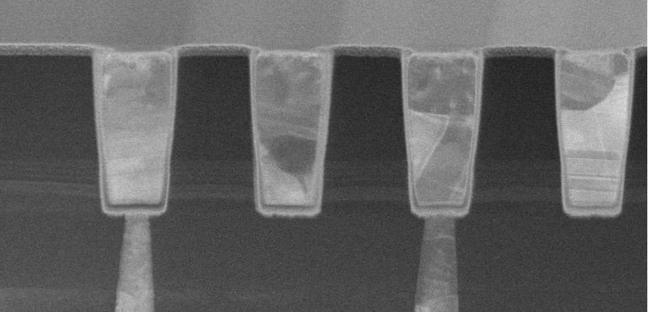
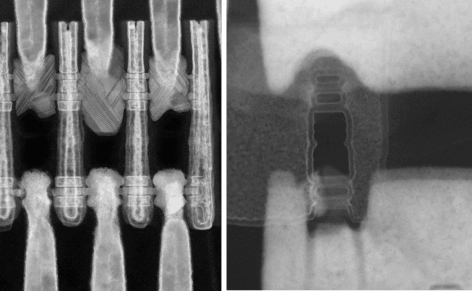
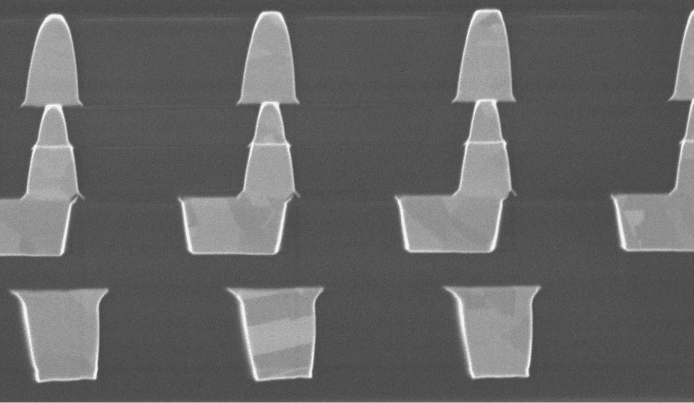
“To enable a BSPDN, a dedicated wafer thinning process (down to a few 100nm) is needed in combination with the ability to process nano-through-silicon vias (n-TSVs) that electrically connect the backside to the frontside of the device wafer. The n-TSVs can either land on the first frontside metal or on a buried power rail (BPR) implemented in the wafer’s frontside.
Imec develops these processes in the frame of its 3D integration program. Our so-called n-TSV-last approach involves bonding the ‘active’ frontside of the first wafer (including the transistors) to a second carrier wafer using a low-temperature wafer-to-wafer bonding technique. The backside of the first wafer is thinned down and the process is completed by n-TSV patterning and tungsten fill, and backside metallization.
One of the challenges relates to the wafer bonding process which inherently induces a distortion of the first wafer. And this challenges the backside lithography step needed to pattern the n-TSVs, more particularly the ability to reach the required alignment accuracy that matches the logic standard cell structure. Imec and its partners develop alternative approaches for enabling better overlay accuracy and for improving the BSPDN.”
Could you elaborate on the added value that imec’s 3D integration technologies have for industry?
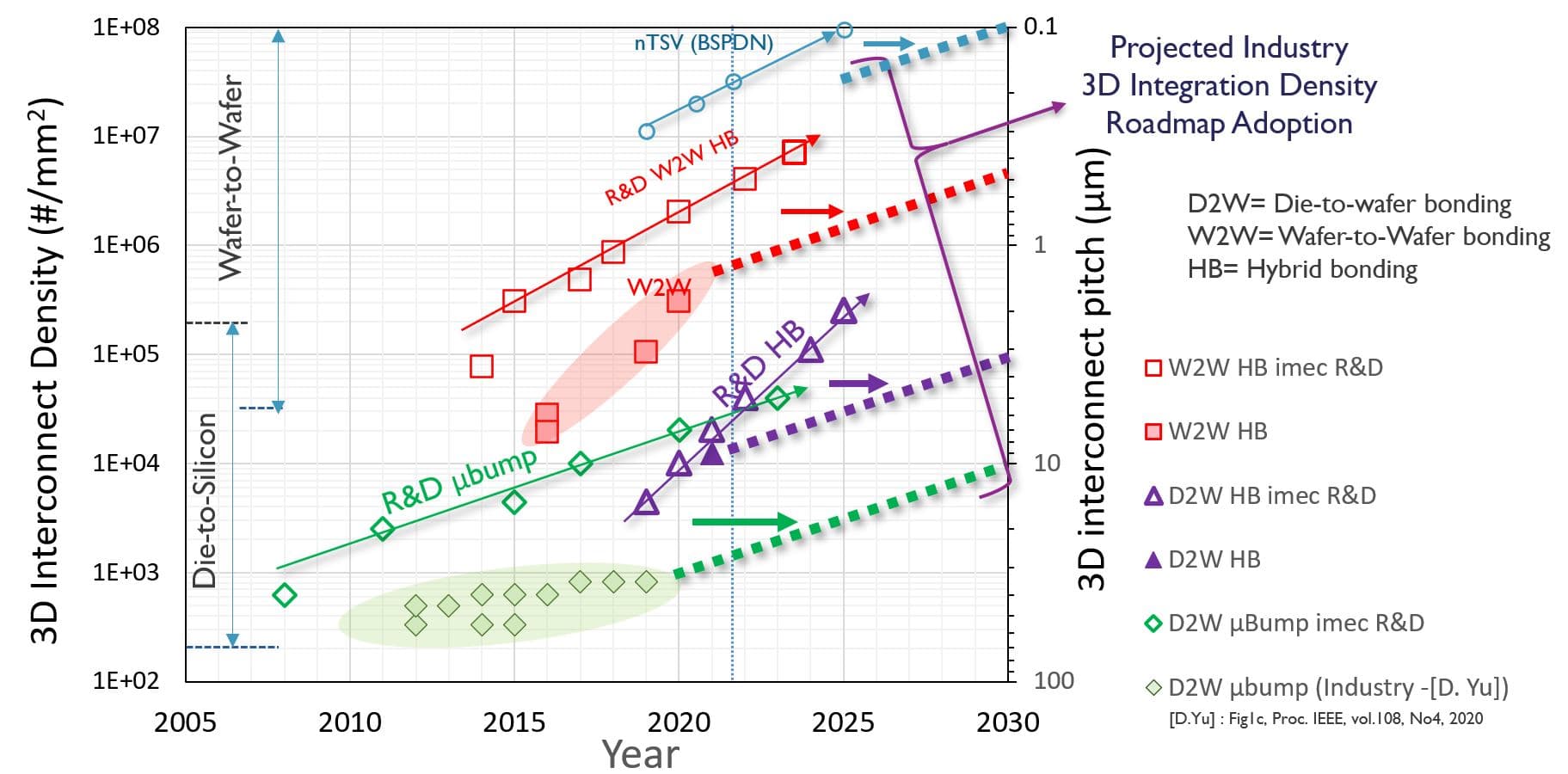
“Today, several commercial ‘3D’ products use a combination of TSVs and Sn microbumps to enable heterogeneous die-to-die or die-to-interposer stacking. While research is showing good promise for scaling TSVs, state-of-the-art Sn microbump pitches in production have however saturated at about 30µm. The problem is the interconnect gap: the die-to-die microbump connection has not caught up to the point where the TSVs can be fully utilized.
At imec, we are pushing the boundaries of what is possible today. We have demonstrated a Sn-based microbump interconnect approach (using damascene under bump metallization) yielding interconnect pitches as low as 7µm and have developed a roadmap for bringing this pitch down to 5µm.
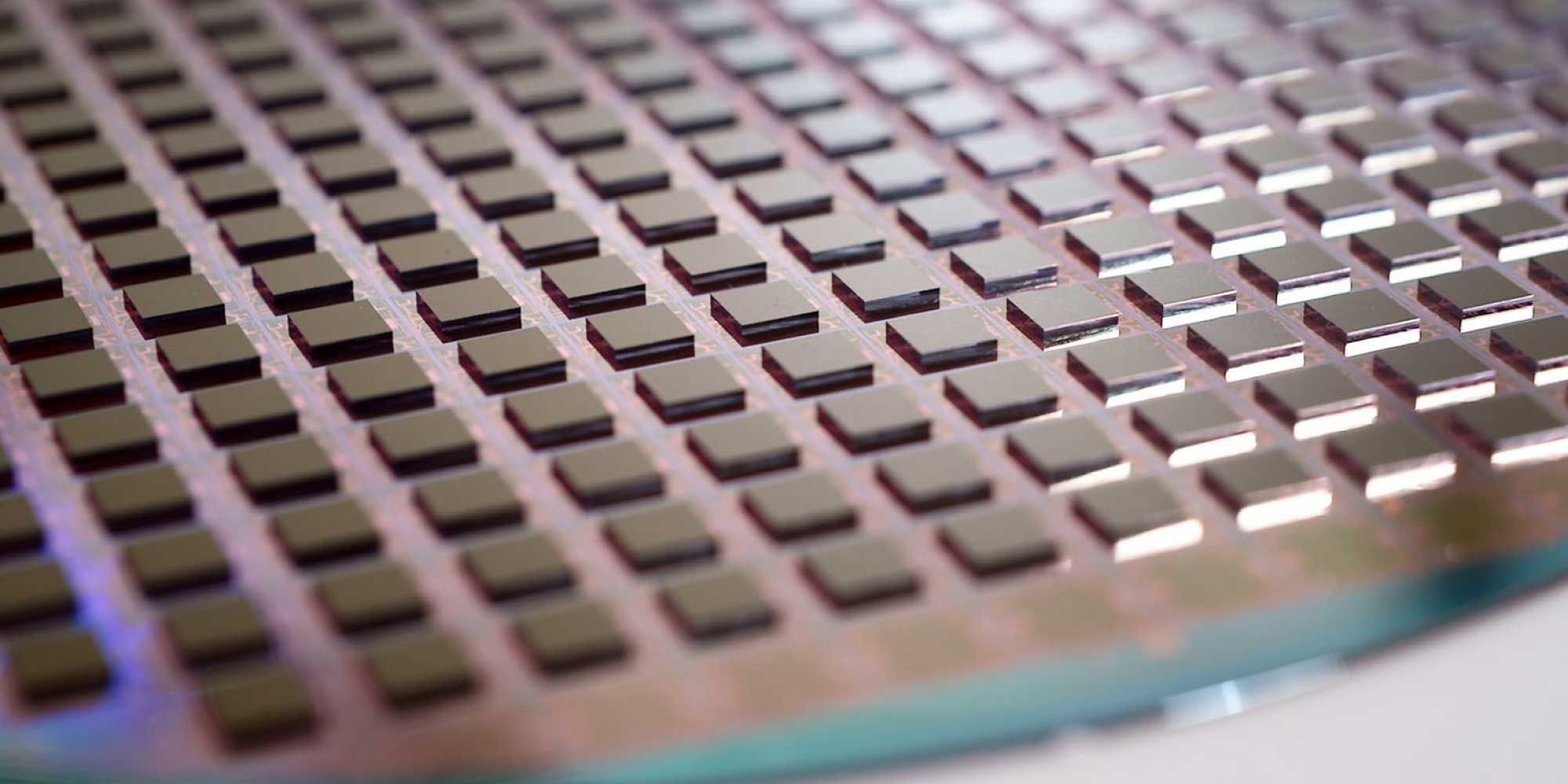
We can further reduce the interconnect pitches (down to 3µm) by using our Cu/SiCN die-to-wafer hybrid bonding approach. Following this approach, dies are stacked using a dielectric-to-dielectric bonding approach, followed by a metal-to-metal connection – without using microbumps. The biggest challenge relates to both the purity and precision with which the dies are to be placed on the wafer.
The highest interconnect densities can be obtained by using our wafer-to-wafer bonding solutions. These developments are driven by memory-on-logic stacking, requiring interconnect pitches far below 1µm. Today, we obtain 700nm pitch and expect to bring this down to an unprecedented 500nm.”
What makes imec’s 3D system integration program unique for the global semiconductor industry?
“Imec proposes a roadmap to the industry of the different 3D integration technologies spanning a range of almost 8 orders of magnitude in 3D interconnect density. Each of these 3D integration technologies serves different needs and therefore targets different end applications such as smartphones, DRAM chips or high-performance compute systems. The optimum choice will be a trade-off between hierarchy-driven 3D interconnect density and the cost of the final solution.
To gain as much benefit as possible at the system level, we continuously push the boundaries of the various options. We do this in tight collaboration with our equipment, metrology and material suppliers, supported by EDA software developers and companies targeting different end applications. This unique ecosystem of partners allows us to accelerate the development of true 3D SOCs, with optimal PPAC gains at the system level.”
This article was originally published in EEWeb.
Want to know more?
Authors

Eric Beyne
Eric Beyne obtained a degree in electrical engineering in 1983 and the Ph.D. in applied sciences in 1990, both from the Katholieke Universiteit Leuven, Belgium. Since 1986 he has been with imec in Leuven, Belgium where he has worked on advanced packaging and interconnect technologies. Currently, he is imec fellow and program director of imec’s 3D system integration program. He received the European Semi Award 2016 for contributions to the development of 3D technologies.
Discover more
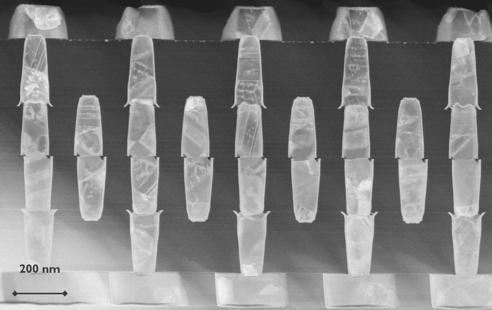
Imec and EV Group demonstrate wafer-to-wafer hybrid bonding with 200nm interconnect pitch and record high overlay accuracy
Read more
IC-Link by imec joins TSMC 3DFabric® Alliance to accelerate advanced packaging and 3D IC innovation
Read more