Cadence Accelerates System Innovation with Breakthrough Integrity 3D-IC Platform
Industry’s first comprehensive 3D-IC platform for multi-chiplet design and advanced packaging
SAN JOSE, Calif., 06 Oct 2021
Highlights:
- Integrity 3D-IC integrates design planning, implementation and system analysis in a single, unified cockpit
- Designers can achieve system-driven PPA through the availability of integrated thermal, power and static timing analysis capabilities
- Cadence’s third-generation 3D-IC solution supports a wide range of application areas, including hyperscale computing, consumer, 5G communications, mobile and automotive
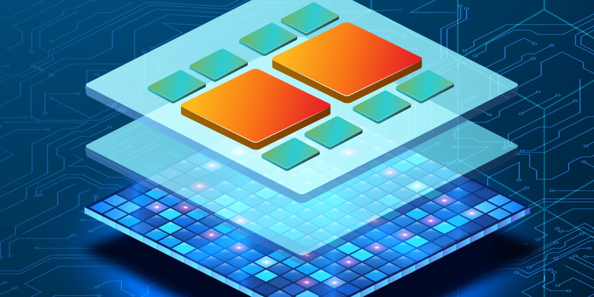
Cadence Design Systems, Inc. (Nasdaq: CDNS) today announced the delivery of the Cadence® Integrity™ 3D-IC platform, the industry’s first comprehensive, high-capacity 3D-IC platform that integrates 3D design planning, implementation and system analysis in a single, unified cockpit. The Integrity 3D-IC platform underpins Cadence’s third-generation 3D-IC solution, providing customers with system-driven power, performance and area (PPA) for individual chiplets through integrated thermal, power and static timing analysis capabilities.
Chip designers creating hyperscale computing, consumer, 5G communications, mobile and automotive applications can achieve greater productivity with the Integrity 3D-IC platform versus a disjointed die-by-die implementation approach. The platform uniquely provides system planning, integrated electrothermal, static timing analysis (STA) and physical verification flows, enabling faster, high-quality 3D design closure. It also incorporates 3D exploration flows, which take 2D design netlists to create multiple 3D stacking scenarios based on user input, automatically selecting the optimal, final 3D stacked configuration. Furthermore, the platform database supports all 3D design types, letting engineers create designs at multiple process nodes simultaneously and perform seamless co-design with package design teams and outsourced semiconductor assembly and test (OSAT) companies that use Cadence Allegro® packaging technologies. For more information on the Integrity 3D-IC platform, please visit www.cadence.com/go/integrity.
Customers using the Integrity 3D-IC platform have access to the following features and benefits:
- Common cockpit and database: Lets SoC and package design teams co-optimize the complete system concurrently, allowing system-level feedback to be incorporated efficiently.
- Complete planning system: Incorporates a complete 3D-IC stack planning system for all types of 3D designs, enabling customers to manage and implement native 3D stacking.
- Seamless implementation tool integration: Provides ease of use through direct script-based integration with the Cadence Innovus™ Implementation System for high-capacity digital designs with 3D die partitioning, optimization and timing flows.
- Integrated system-level analysis capabilities: Enables robust 3D-IC design through early electrothermal and cross-die STA, which allows early system-level feedback for system-driven PPA.
- Co-design with the Virtuoso® Design Environment and Allegro packaging technologies: Allows engineers to seamlessly move design data from Cadence analog and packaging environments to different parts of the system through the hierarchical database, enabling faster design closure and improved productivity.
- Easy-to-use interface: Includes a powerful user cockpit with a flow manager that provides designers with a uniform, interactive way to run relevant system-level 3D system analysis flows.
“Cadence has historically offered customers strong 3D-IC packaging solutions through its leading digital, analog and package implementation product lines,” said Dr. Chin-Chi Teng, senior vice president and general manager in the Digital & Signoff Group at Cadence. “With recent developments in advanced packaging technologies, we saw a need to further build upon our successful 3D-IC foundation, providing a more tightly integrated platform that ties our implementation technology with system-level planning and analysis. As the industry continues to move toward different configurations of 3D stacked dies, the new Integrity 3D-IC platform lets customers achieve system-driven PPA, reduced design complexity and faster time to market.”
The Integrity 3D-IC platform is part of the broader Cadence 3D-IC solution portfolio, which goes beyond digital and includes system and verification and IP features. The broader solution provides hardware and software co-verification and power analysis of the full system via the Dynamic Duo, which consists of the Palladium® Z2 and Protium™ X2 platforms. It also provides connectivity via chiplet-based PHY IP with PPA optimized for latency, bandwidth and power. The Integrity 3D-IC platform offers co-design capabilities with the Virtuoso Design Environment and Allegro technologies, integrated IC signoff extraction and STA with the Quantus™ Extraction Solution and Tempus™ Timing Signoff Solution, and integrated signal integrity/power integrity (SI/PI), electromagnetic interference (EMI) and thermal analysis with the Sigrity™ technology portfolio, Clarity™ 3D Transient Solver and Celsius™ Thermal Solver. Both the new Integrity 3D-IC platform and the broader 3D-IC solution portfolio are built on a solid foundation of SoC design excellence and system-level innovation, supporting the company’s Intelligent System Design™ strategy. For more information on the Cadence 3D-IC solution, visit www.cadence.com/go/3DIC.
Endorsements
“With 3D-IC design continuing to gain momentum, there is an increased need to automate the planning and partitioning of a 3D stack die system more efficiently. As the world-leading research and innovation hub in nanoelectronics and digital technologies and through our longstanding collaboration with Cadence, we’ve successfully found automated ways to partition designs to build an optimal 3D stack with increased accessible memory bandwidth that pushes performance and lowers power in advanced-node designs. The integrated memory on the logic flow included in Cadence’s Integrity 3D-IC platform enables cross-die planning, implementation and multi-die STA, which our research teams demonstrated on a multi-core high-performance design.”
-Eric Beyne, senior fellow and program director, 3D System Integration, imec
“To push AI acceleration using optical computing, we’ve consistently leveraged all the latest, innovative trends in the chip design industry—a key innovation being multi-chiplet stacking. In order to build a heterogeneous multi-chiplet stacked design, it is important to have a fully integrated planning and implementation system, which can represent multiple technology nodes in a single cockpit. The Cadence Integrity 3D-IC platform provides a unified database solution with implementation and early system-level analysis capabilities, including timing signoff and electrothermal analysis. It helps us deliver next-generation innovation using optical computing for AI acceleration.”
– Ph.D Yichen Shen, founder and CEO of Lightelligence Inc.
“There are increased requirements for building 2.5D/3D-IC designs with multiple chiplets like logic dies and high-bandwidth memories that are connected with silicon interposer technology. To meet our performance criteria, interposer routing needs automation to be correct-by-construction while taking into account location, shielding and system integrity requirements. The Cadence Integrity 3D-IC platform is well integrated for optimal interposer implementation and system analysis and offers fast, complete system analysis, enabling us to deliver designs that meet memory bandwidth demands for hyperscale computing and 5G communications.”
-Tuobei Sun, R&D head, Department of Packaging and Testing, SaneChips
More information about the Integrity™ 3D-IC platform can be found in Cadence's press release.
About Cadence
Cadence is a pivotal leader in electronic design, building upon more than 30 years of computational software expertise. The company applies its underlying Intelligent System Design strategy to deliver software, hardware and IP that turn design concepts into reality. Cadence customers are the world’s most innovative companies, delivering extraordinary electronic products from chips to boards to systems for the most dynamic market applications, including consumer, hyperscale computing, 5G communications, automotive, mobile, aerospace, industrial and healthcare. For seven years in a row, Fortune magazine has named Cadence one of the 100 Best Companies to Work For. Learn more at cadence.com.
Discover more



Imec and Diraq demonstrate first coherent operation of eight silicon MOS spin qubits fabricated in a 300mm CMOS-compatible foundry process
Read more


Neural telemetry breakthrough: new chip delivers ten-fold compression while preserving signal integrity
Read more

