Towards efficient ESD protection strategies for advanced 3D systems-on-chip
Guidelines for protecting the internal I/O interfaces from electrostatic discharge during die or wafer bonding steps
In short
The continuous scaling of interconnect densities in 2.5D/3D technologies leaves little room for implementing ESD protection circuits at the internal I/O interfaces.
This forces industry to invest more heavily in ESD prevention during die-to-die and die-to-wafer bonding steps, and to avoid over-design of the ESD protection circuits.
Doing that in the most efficient way requires a more fundamental understanding of the ESD events that happen at the internal I/O interfaces.
This article presents useful insights, translated into practical guidelines and research directions for circuit designers and bonding tool suppliers.
ESD protection strategies for monolithic systems-on-chip
Failures caused by electrostatic discharges (ESD) are an ongoing concern for the semiconductor industry. ESD events can affect electronic products at any point during manufacturing and assembly, and during transportation and use of the product. ESD discharges happen in a very short timeframe (pulse widths ranging from below 1ns to 200ns, and rise times from below 200ps to 10ns). In this short period of time, excess currents in the order of 0.1 – 10A might run through the IC and package, damaging the chip by causing metal interconnect burnout or gate oxide breakdown.
Not surprisingly, the industry is heavily committed to safeguard electronic products, focusing on both prevention and protection. To prevent ESD events as much as possible, IC manufacturing and assembly happen in ESD-controlled facilities, where appropriate materials are being used, and operators and equipment are properly grounded. Prevention is complemented by adding on-chip protection circuitry. These circuits shield the chip’s input and output interfaces (I/O) that connect the chip to the outside world. When an ESD event hits the chip, these circuits ensure a safe, low-resistive discharge path to the ground, while limiting voltages to a safe level.
For monolithic systems-on-chip, ESD design strategies are clearly defined and evolve with every new technology that enters the technology roadmap [1]. To qualify the chip’s robustness to ESD events, the semiconductor industry uses two ESD control standards, that are representative of the most common ESD events: the human body model (HBM) and the charged device model (CDM). While HBM represents the discharge from a human being (and, by extension, from other external objects) to an IC, CDM captures what happens when the chip itself is charged and discharges to the environment. The industry also sets ESD target levels for various electronic products. Today, monolithic systems-on-chip used in high-performance computing applications are qualified for 125V or 250V CDM, depending on customer demands. For HBM, the specs range between 100V and 500V, depending on the functionality of the I/O pins and customer demands.
2.5D/3D technologies: internal I/O interfaces add to the complexity
Advanced computing systems are increasingly evolving from monolithic planar systems-on-chip towards multi-die heterogeneous systems, where 2.5D and 3D interconnect technologies are used to stack and interconnect the different dies or tiers. A large variety of 3D interconnect technologies has been developed over the years, offering a broad range of interconnect densities, and serving different applications. They include for example 2.5D interposer technology (where dies are placed next to each other, connected through an (active) interposer), and microbump or hybrid bonding approaches for either die-to-wafer or wafer-to-wafer stacking.
From ESD point of view, 2.5D and 3D technologies introduce an additional complexity. Once packaged, the 3D-stacked system still features I/O pins that connect the overall system to the outside world. Just like for packaged single dies, these external I/O circuits can be electrostatically discharged to and from external objects or humans, and comparable ESD control standards as defined for monolithic ICs remain valid.
But on top of that, 3D-stacked systems contain internal I/O circuits that interface between the different dies of the stack, without any connection to package pins. These interfaces are only vulnerable to ESD events that occur during die or wafer stacking, for example during die pick-up, die transfer, and die or wafer bonding processes. Therefore, it is important for 2.5/3D technologies that ESD events are suppressed as much as possible during stacking and assembly. Should they occur, chip manufacturers must ensure that the internal I/O pins are sufficiently protected without affecting their performance.
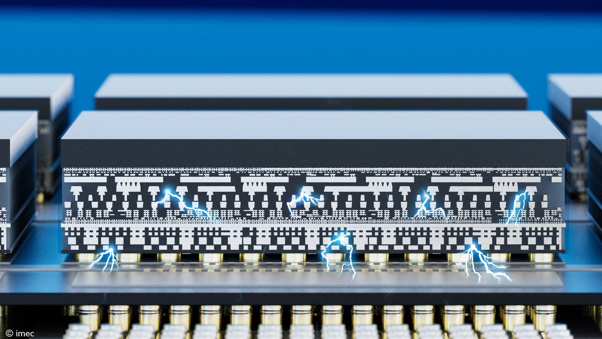
The scaling of 3D interconnect densities drives the need for 0V ESD protection
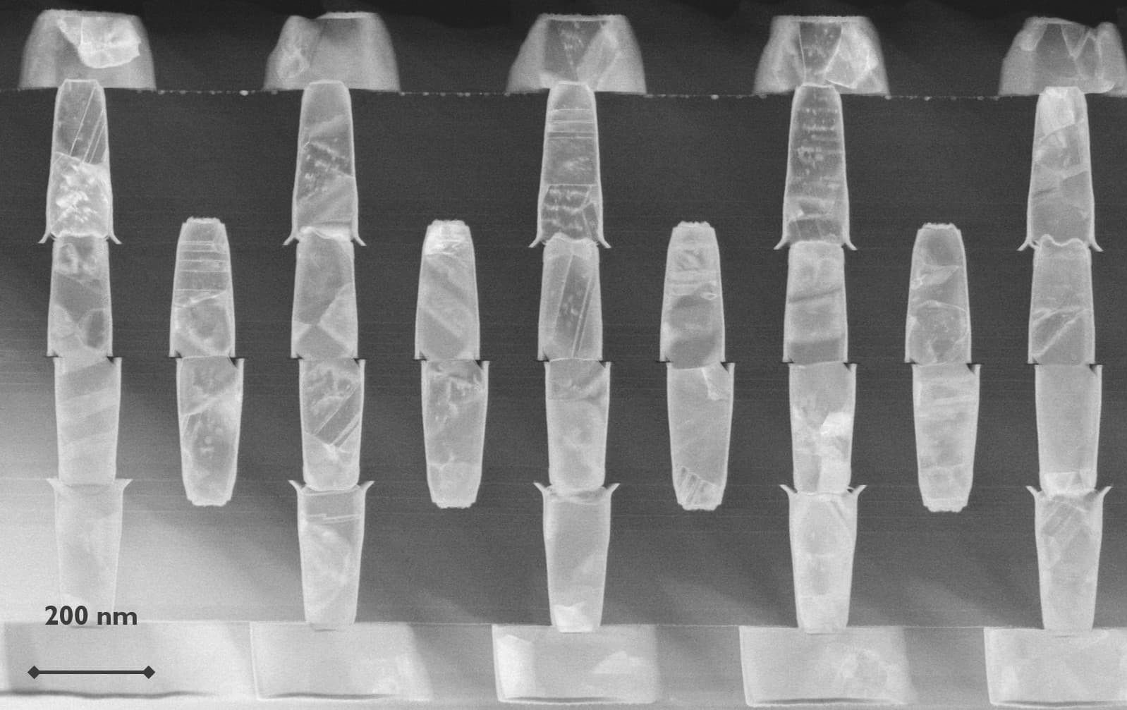
But the continuing increase in 3D interconnect densities complicates the protection of the internal interfaces. Industry is pushing each of the 3D interconnect technologies towards finer grained interconnects, targeting for example logic/memory-on-logic type of stacking applications. Researchers at imec recently demonstrated die-to-wafer hybrid bonding with interconnect pad pitches as small as 2µm. For wafer-to-wafer hybrid bonding, an interconnect pitch of just 400nm has been achieved, translating in over a million Cu interconnects per mm2 at the surface of the dies. [2, 3]
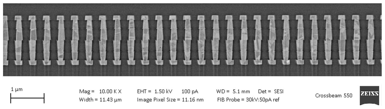
The downside of this evolution? Less and less space becomes available for protection circuits that shield the internal I/O circuits from ESD during bonding. Eventually, we expect that there will be no space at all. This forces designers to increasingly smaller ESD protection circuits at the I/O interfaces. This, however, reduces the ESD robustness of the internal I/O pins during stacking and assembly. That is why the ESD community is increasingly promoting the prevention of ESD events during bonding, ultimately eliminating the need for ‘internal’ ESD protection circuits wherever possible.
Less ESD protection not only means less area consumption: it also benefits the performance of the I/O circuits. ESD protection circuits can directly reduce the performance of the circuits they try to protect because of the added parasitic capacity. Adding ESD protection therefore has become a tradeoff between robustness and performance.
A call for enhanced fundamental understanding of ESD
Moving towards 0V ESD protection requires in-depth knowledge of the ESD events that could hit the I/O internal pins during bonding. For ‘standard’ monolithic ICs, ESD protection is relatively well understood. But for internal I/O interfaces in 2.5D/3D technologies, the impact of ESD events is not yet as clear. Today, no standard is available that describes the requirements and target levels for ESD protective measures in 2.5D/3D bonding technologies. As repeatedly reported at ESD related conferences and workshops, the conventional assumptions for testing seem not to apply to advanced bonding technologies and internal pins. Measurements suggest that after an ESD event, ESD pulses behave differently in terms of peak current, pulse width and rise time than what is assumed in, for example, standard CDM testing.
This calls for more fundamental understanding. Quantifying how critical ESD events are to internal interfaces will provide guidance for setting up industry target levels and help foundries take precautions. In addition, modeling the ESD events and the breakdown mechanisms will help designers to adjust their ESD protection circuit designs.
Invest in prevention, avoid over-design, and follow a customized approach
At imec, a team of researchers combines experiments and modelling to unravel the breakdown mechanisms that follow an electrostatic discharge during die-to-wafer or wafer-to-wafer stacking. They investigate for example how the gate oxide of the internal I/O devices breaks down in the absence of ESD protection circuits. In addition, they study the ESD pulse shape in the presence of ESD protection circuits. Looking into the various parameters affecting the ESD pulse shape will help designers make the protection circuits more efficient, in cases where ESD discharges cannot completely be avoided. First insights have been presented at the 2024 VLSI Conference [4].
The results of these and other studies – as reported e.g. to the Industry Council on ESD target levels [5] – can be translated into guidelines and research directions to the broader ESD ecosystem.
1. The voltage suppression effect reduces the need for ESD protection circuits
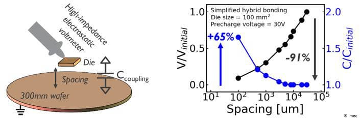
Without ESD protection circuits in internal I/O pins, even a very low ESD voltage may break the sensitive internal I/O circuits. Fortunately, during the bonding step, an important effect plays to our advantage: the voltage suppression effect. During die-to-wafer or wafer-to-wafer bonding, the die/wafer and the target wafer can be considered a parallel plate capacitor. Following the laws of physics, its capacitance increases due to the reduced spacing when the die/wafer moves closer to the target wafer. This, in turn, significantly reduces the threatening electrostatic voltage.
Imec researchers confirmed the effect in simplified hybrid bonding experiment setups. The measurements indicate that the effect is far more pronounced for wafer-to-wafer bonding than for die-to-wafer bonding configurations. Although preliminary results suggest that ESD protection might be unnecessary in wafer-to-wafer bonding, further research is needed to find out how strong the effect will be in ‘real-life’ bonding processes.
2. Call out to bonding tool developers: bring ESD prevention inside the bonding tools
As learned from the above experiments, several factors influence the effectiveness of the voltage suppression effect. One of these is the parasitic capacitance from the die or wafer holder. This indicates that the bonding tool itself can play a critical role in ESD prevention, for example by minimizing parasitic capacitance from the holder. Another example is the incorporation of custom air ionization solutions into die-to-wafer assembly tools, which can help to discharge the dies safely inside the tool.
3. The series resistance from the protective circuit needs to be considered when designing ESD protection circuits
In case external ESD control measures cannot completely prevent breakdown, internal ESD protection circuits are essential to drain the ESD current. As explained before, the available space for these circuits becomes limited. But several considerations can help avoid over-design, and, as such, reduce area consumption and maintain the performance of the internal I/O circuits.
The imec team has analyzed the ESD pulse shape after an ESD event hits the protection circuit. They observed a fast rise time of the ESD pulse (down to 22ps), much faster than the typical CDM pulse. In addition, the series resistance arising from the interconnect metal lines and the ESD protection devices themselves significantly impacts the ESD pulse shape. Narrow interconnect lines with a higher series resistance for example tend to have a positive effect on the ESD pulse shape, translating into slower CDM discharges and smaller peak currents.
These observations imply that the characteristics of the ESD pulse and the circuit’s series resistance may not be overlooked when designing ESD protection circuits for 2.5/3D technologies. If not considered, this could lead to excessive ESD protection, resulting in unnecessary use of the Si area and performance degradation of the internal I/O pins. On the other hand, increasing the series resistance where possible would reduce the needed size of ESD protection circuits.
4. 3D systems-on-chip need a customized approach to ESD protection
We already mentioned that the voltage suppression effect may eventually rule out the need for implementing ESD protection circuits at the I/O interfaces in wafer-to-wafer bonding configurations. For die-to-wafer bonding processes, where the need for ESD protection will be higher, our measurements indicate that the size of the dies also plays a critical role in the occurrence of a/extent of the ESD event. Die size will therefore also be a knob in designing the protection circuit.
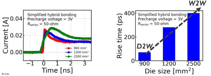
Overall, 3D systems-on-chip need a customized approach to ESD protection. Distinct design strategies are needed for the different bonding technologies, and for different die sizes in case of die-to-wafer bonding. More research is needed to investigate the specific needs of microbump and hybrid bonding approaches, for both die-to-wafer and wafer-to-wafer technologies.
5. Measurements confirm the need for new standards
When ESD events occur at the I/O interfaces of bare chips and wafers, ESD pulses are observed to behave differently than what is assumed within the constraints of the conventional standards, written for packaged chips. Our measurements confirm the need for developing new standards that define the requirements for testing.
Conclusion and outlook
The continuous scaling of the interconnect densities offered by various 2.5D/3D technologies challenges the ESD protection of internal I/O interfaces during stacking. For future 3D systems-on-chip, there will hardly be any space available for implementing ESD protection circuits, justifying the need to invest more heavily in ESD prevention. In cases where protection circuits will still be needed, several design factors can be considered that help avoid over-design of the protection circuits. Overall, each of the 3D interconnect technologies might require a different approach to ESD protection and prevention.
Imec, in close collaboration with the ESD Association, continues its research efforts in developing 3D-specific ESD protection strategies. In the longer term, the collaborative efforts are expected to lead to new standards for testing and qualifying the ESD robustness of advanced 2.5/3D technologies.
This article was originally published in Nature Review Electrical Engineering.
Want to know more?
[1] ‘How to protect advanced CMOS technologies with thin Si substrates against ESD events’, imec Reading Room, February 2024
[2] ‘Imec demonstrates die-to-wafer hybrid bonding with a Cu interconnect pad pitch of 2µm’, imec press release, May 2024
[3] ‘Wafer-to-wafer hybrid bonding: pushing the boundaries to 400nm interconnect pitch’, imec Reading Room, February 2024
[4] ‘Toward 0V ESD protection in 2.5D/3D advanced bonding technology’, S.H. Lin et al., VLSI 2024
[5] Industry council on ESD target levels, WP 2, part II, revision 1.1, year 2023
Authors

Shane (Shih-Hsiang) Lin
Shih-Hsiang Lin received his B.Sc. degree in electrical engineering from National University of Kaohsiung (NUK), Kaohsiung, Taiwan, in 2018, and his M.Sc. degree from National Cheng Kung University (NCKU), Tainan, Taiwan, in 2021. In addition, he spent one year as an intern at imec in 2021. He joined the department of electronics and informatics (ETRO) at the Vrije Universiteit Brussel (VUB) and the Electrostatic discharge (ESD) team at imec, Belgium, in 2021, where he is pursuing his PhD degree. His current research topic is ESD risk investigation in three-dimensional (3D) technologies.

Marko Simicic
Marko Simicic received the B.Sc. and M.Sc. degrees in electrical engineering and information technology from the University of Zagreb, Croatia, in 2010 and 2012 respectively. He obtained a PhD degree from the department of electrical engineering ESAT, KU Leuven, Belgium in 2018. In 2017 he joined the ESD team in imec, Belgium. He is a certified ESD control program manager since 2022. He has authored or co-authored more than 35 papers in international journals and conference proceedings. His current research area is rather wide and includes ESD device and circuit design in advanced semiconductor and 3D/2.5D stacking technologies, novel ESD testing and ESD control process assessment.

Nicolas Pantano
Nicolas Pantano is a Principal Member of Technical Staff at imec. He obtained his B.Sc. and M.Sc. degrees in electrical engineering from the University of Brussels, Belgium, in 2010 and 2012, respectively. In 2021, he completed his PhD degree from the Department of Electrical Engineering ESAT, KU Leuven, Belgium. Additionally, he received an M.Sc. in Business Administration and Finance from the Solvay Business School, Belgium, in 2015. In 2013, he joined imec in the 3D and Silicon Photonics department. His research focuses on electrical and optical interconnects for 2.5D/3D integrated systems for applications including mobile, high-performance computing, AI, and automotive. He has authored more than 21 publications in journals and conference proceedings.
Discover more
Imec and EV Group demonstrate wafer-to-wafer hybrid bonding with 200nm interconnect pitch and record high overlay accuracy
Read more
IC-Link by imec joins TSMC 3DFabric® Alliance to accelerate advanced packaging and 3D IC innovation
Read more