Wafer-to-wafer hybrid bonding: pushing the boundaries to 400nm interconnect pitch
Innovations in Cu/SiCN bonding technology are driven by memory-on-logic stacking needs

In short
Wafer-to-wafer hybrid bonding is an attractive 3D integration technology for stacking multiple heterogeneous chips with high 3D interconnect density.
To expand the application domain towards, e.g., memory-on-logic stacking, the 3D interconnect pitch must scale far below 1µm – today’s state of the art.
This article highlights recent design and technology innovations that have enabled hybrid Cu & silicon-carbon-nitride (SiCN)-to-Cu & SiCN bonding with interconnect pitches down to an unprecedented 400nm.
The promise of wafer-to-wafer hybrid bonding
3D integration is a crucial technology to realize multi-chip heterogeneous integration solutions, the industry’s response to the demand for ever higher power, performance, area, and cost gains at the system level. 3D stacking is being introduced at different levels of the electronic system hierarchy, from the package level to the transistor level. As a result, a large variety of 3D interconnect technologies have been developed over the years, spanning a broad range of interconnect pitches (from mm to less than 100nm) and serving different application needs. This ‘3D interconnect landscape’ is illustrated in the figure below. The landscape is highly dynamic, with each technology scaling to smaller interconnect pitches in time. Near the end of this technology ‘spectrum’, we find wafer-to-wafer hybrid bonding, promising high interconnect densities and small interconnect parasitics. This ‘hybrid’, Cu-to-Cu & dielectric-to-dielectric, bonding technique uses Cu damascene technology to define the bonding surfaces, potentially allowing for very fine pitch scaling.
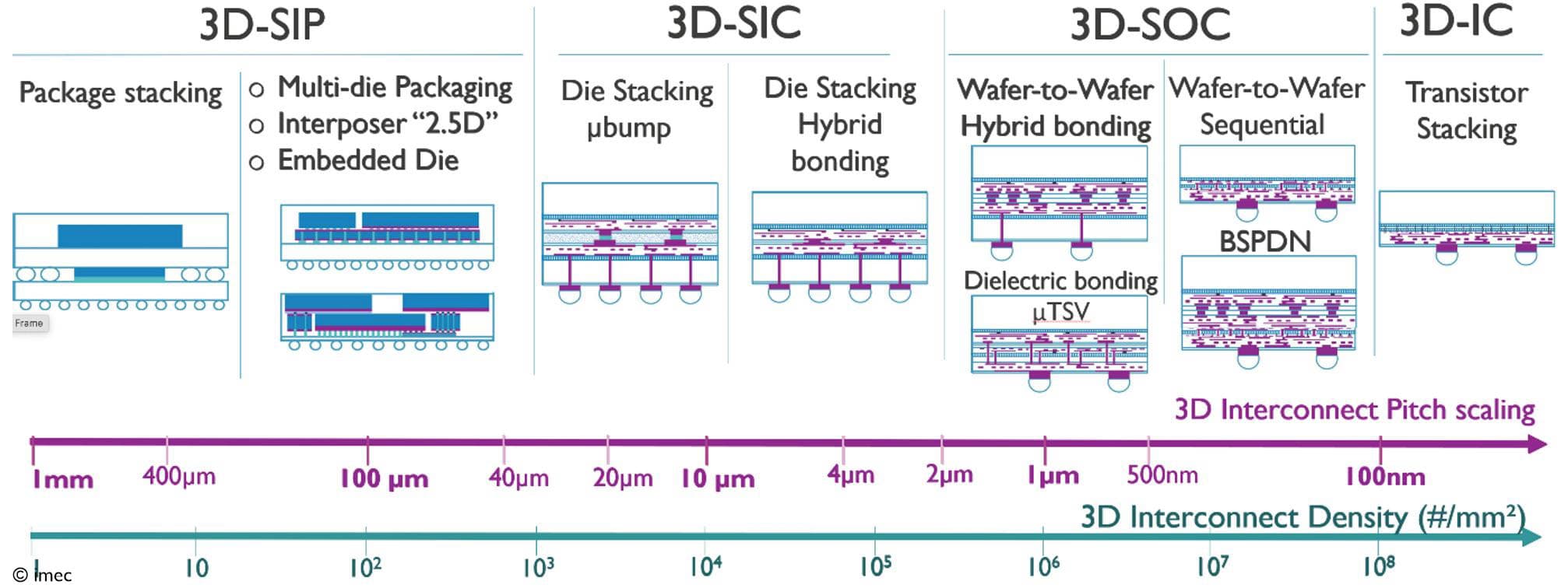
Until recently, high-volume manufacturing of wafer-to-wafer hybrid bonding was mainly limited to the field of stacked image sensors on signal-processing circuit layers. More recently, the technique is being adopted to integrate CMOS peripheral circuitry on top of 3D NAND layers. These commercial applications take advantage of the technology’s ability to integrate a million interconnects per mm2, enabled by a tight Cu interconnect pitch of about 1µm. Another asset of the technology is the possibility to ‘mix and match’ different materials and functionalities and CMOS technologies of different generations.
In the years to come, we expect the application domain to expand significantly. With the aid of system technology co-optimization (STCO), circuit partitioning will happen at an ever-lower level of the design hierarchy – think of circuit blocks or even standard cells. We are seeing the first announcements of memory-on-logic applications – SRAM on top of logic, for example – which have been one of the main drivers for developing advanced wafer-to-wafer hybrid bonding technologies. To fully exploit the potential of wafer-to-wafer hybrid bonding in these cases, researchers must succeed in scaling the interconnect pitch far below 1µm.
Current process flow for wafer-to-wafer hybrid bonding
Today’s wafer-to-wafer hybrid bonding process flows start from two fully processed 300mm wafers, with completed front-end-of-line (FEOL) and back-end-of-line (BEOL). The first part of the flow resembles an on-chip BEOL damascene process, where small cavities are etched into the bonding dielectric – for which SiO2 is predominantly used. The cavities are filled with barrier metal, seed, and Cu. This is followed by a chemical mechanical polishing (CMP) step optimized for high across-wafer uniformity to produce extremely flat dielectric surfaces while achieving a few nanometers of recess for the Cu pads. After accurate alignment, the actual bonding of the two wafers is performed at room temperature by bringing the wafers into contact in the center of the wafer. The polished wafer surfaces adherence results in a strong wafer-to-wafer attraction, resulting in a bonding wave, closing the wafer-to-wafer gap from the center to the edge. After this room temperature bonding step, the wafers are annealed at higher temperatures to obtain a permanent dielectric-to-dielectric and Cu-to-Cu bond.
Emerging applications challenge current process steps
With the expansion of the application domain, more advanced implementations of hybrid bonding are emerging. As explained before, there is a trend to bring the bonding process closer and closer to the front end to enable, for example, logic-on-logic or memory-on-logic stacking. This requires not only finer interconnect pitches, but also involves more post-processing after the bonding step.
One very specific example is a backside power delivery network (BSPDN), for which wafer-to-wafer bonding is a critical step. In BSPDN processing, the front side of the first wafer is bonded to a carrier wafer. The backside of the first wafer is then thinned down, and the process is completed by n-TSV patterning, metal fill, and backside metallization. In this example, part of the BEOL processing – i.e., integrating the ‘fattest’ interconnect lines that serve the power delivery – is carried out after the wafer bonding process.
These applications raise more stringent scaling needs that challenge the current process flow. The main pitfalls relate to the Cu-to-Cu alignment accuracy, wafer purity and topology before bonding, and bond strength of the dielectrics and Cu pads at small interconnect pitches.
Improving the wafer-to-wafer hybrid bonding process to enable 400nm pitch interconnects
At the 2023 IEEE International Electronic Devices Meeting (IEDM 2023), imec reported important innovations that have paved the way to an unprecedented 400nm interconnect pitch. The work results from a comprehensive study that examined various aspects of wafer-to-wafer hybrid bonding [1].
Design improvements to compensate for scaling and alignment limitations
Imec researchers proposed a test vehicle design with a hexagonal grid and circular Cu pads for the first time instead of the traditional square grid with a square or circular pad design. The new design offers several advantages. It allows the Cu pads to be packed in the densest way possible, with equal distances between all neighboring pads. Consequently, with further scaling, such a configuration makes it easier to control the Cu pad density while maximizing the Cu pad size and spacing. The team is also investigating the impact of using either an equal or an unequal pad design. In the latter case, the top wafer is designed with smaller critical Cu pad dimensions than the bottom wafer. Unequal pad designs offer a few advantages, including more significant bonding overlay tolerance, reduced parasitic capacitance and higher dielectric breakdown strength at small interconnect pitches.
Accurate control of the surface topography
Before the two wafers are bonded, the surfaces of both wafers must be extremely flat and clean to achieve a reliable hybrid bonding process. CMP, therefore, is a very demanding process step. It also ensures uniformrecess of the Cu pads, meaning that the Cu remains a few nanometers below the dielectric surface prior to the bonding. This is required to obtain void-free bonding after anneal. By combining an advanced CMP process with dummy pads in the layout design, the researchers succeeded at accurately controlling the Cu pad height and surface topology over the entire wafer.
SiCN dielectric for better bond strength and scalability
Imec previously proposed SiCN as the dielectric of choice for small interconnect pitches. SiCN surfaces exhibit a higher bonding energy as compared to SiO2 surfaces – meaning that it takes more energy to break the bond. Also, SiCN acts as a diffusion barrier for Cu and a wafer passivation layer, blocking gas diffusion, resulting in a more thermally stable bonding interface. These properties are of increasing importance when scaling the hybrid bond interconnect pitches. Measurements based on nanoindentation – an emerging technique for evaluating bond strengths – confirmed that the SiCN-SiCN bond strength significantly outperforms the SiO2-SiO2 bond strength. The high bond strength can be obtained after post-bonding anneal at only 250°C and does not degrade at higher temperatures.
400nm pitch interconnects with excellent electrical performance
The above insights were used to perform an advanced wafer-to-wafer Cu/SiCN bonding process. The actual bonding was performed with a commercial high-quality wafer bonder equipped with advanced alignment capabilities – a tool critical to the success of the process. 300mm wafers were successfully bonded, yielding Cu interconnects with an unprecedented 400nm pitch.
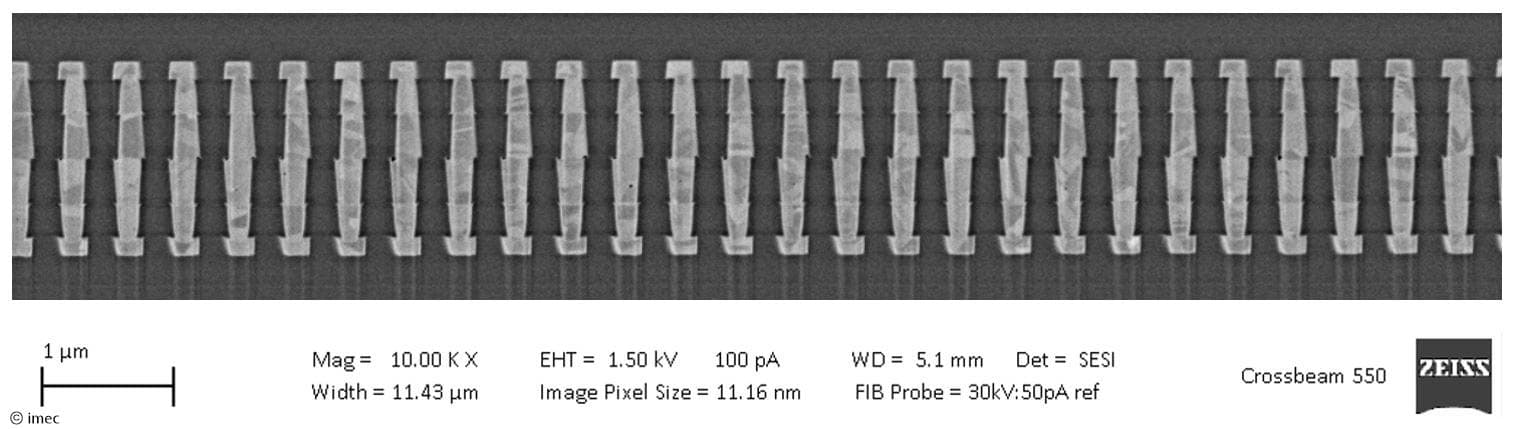
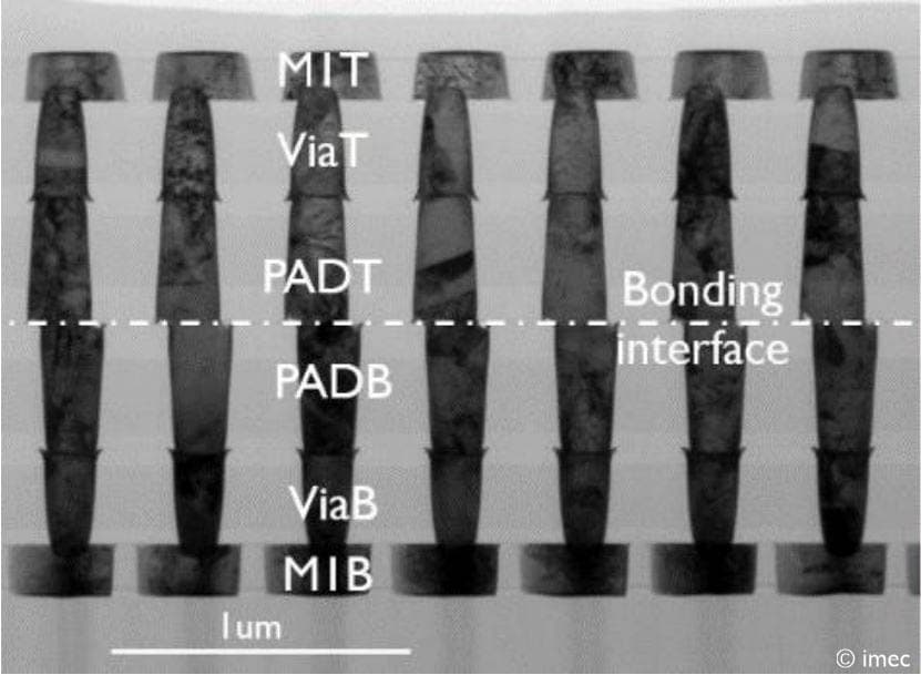
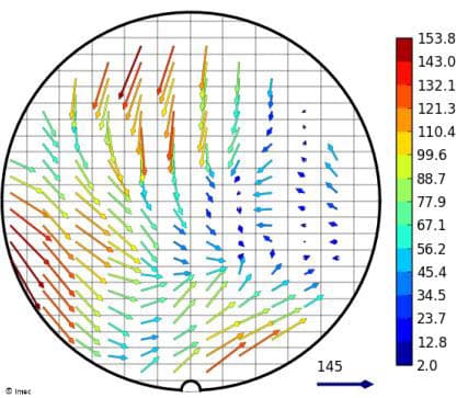
The results show successful control of the Cu/SiCN surface topography, precise alignment (resulting in overlay below 150nm), and favorable electrical performance (i.e., low single contact resistance).
The need for <100nm overlay control
For the first time, the team also investigated the relation between bonding overlay and reliability (i.e., dielectric breakdown and yield). The results confirm a higher dielectric breakdown strength of unequally designed Cu pads than equal pads at small interconnect pitches. The team also concluded that for these 400nm interconnect pitches, overlay control needs to be smaller than 100nm to have sufficient yield in high-volume manufacturing. Therefore, meeting the needs of future 3D-SOC designs imposes intense demands on the overlay accuracy of next-gen wafer bonding equipment.
Conclusion
Wafer-to-wafer hybrid bonding has emerged as a promising 3D integration technology to enable ever-increasing I/O density and more efficient connections between functional dies. To enable applications like memory-on-logic – where wafer-to-wafer bonding happens close to the front end – the scaling of the Cu interconnect pitch must be pushed to its ultimate limits. Improvements in grid design, enhanced control of the surface topography, the use of SiCN as a dielectric, fundamental understanding of the bonding mechanisms, and improved overlay control are identified as key enablers to realize electrically functional and reliable Cu interconnects at 400nm (and below) pitch. These results provide the groundwork for developing future wafer-to-wafer bonding processes with even smaller interconnect pitches.
This article was originally published in Nature Review Electrical Engineering.
Want to know more?
[1] ‘The challenges of Cu/SiCN wafer-to-wafer hybrid bonding scaling down to 400nm pitch,’ S.A. Chew et al., IEDM 2023;
Interested in receiving this article? Fill in our contact form.
Authors

Soon Aik Chew
He obtained a B. Eng. (Materials) from the Universiti Sains Malaysia in 2001 and an M.Sc. in Electrical and Electronics Engineering from the Universiti Teknologi PETRONAS in 2004. Before joining imec, he worked on process and device development with ASE, Silterra, SSMC and Altera (now part of INTEL PSG). He has been with imec since Sept. 2011, working on CMOS device middle-of-line (MOL) technologies; his current research focuses on wafer-to-wafer hybrid bonding technologies.

Joeri De Vos
Joeri De Vos is heading the 3D integration team at imec. He obtained a degree in electrical engineering in 1991 and a Ph.D. in Applied Sciences in 1999, both from the University of Ghent, Belgium. He has been with imec since 2000 with many years of experience in integrating flash memory, CMOS imagers and 3D demonstrators. The 3D integration team he leads focuses on scaling wafer-to-wafer hybrid bonding, BSPDN, and interposer technology.

Eric Beyne
Eric Beyne obtained a degree in electrical engineering in 1983 and the Ph.D. in applied sciences in 1990, both from the Katholieke Universiteit Leuven, Belgium. Since 1986 he has been with imec in Leuven, Belgium where he has worked on advanced packaging and interconnect technologies. Currently, he is imec fellow and program director of imec’s 3D system integration program. He received the European Semi Award 2016 for contributions to the development of 3D technologies.
Discover more



Sony and imec unveil high-density backside connectivity module enabling next-generation 3D chip integration
Read moreASML, TSMC and imec bring industry-ready 2D-material transistors closer with breakthrough 300mm integration
Read more
Imec and EV Group demonstrate wafer-to-wafer hybrid bonding with 200nm interconnect pitch and record high overlay accuracy
Read more