IC-Link by imec joins TSMC 3DFabric® Alliance to accelerate advanced packaging and 3D IC innovation
Expands global ASIC services expertise and aims to take on the industry’s most advanced AI, HPC, mobile and automotive projects
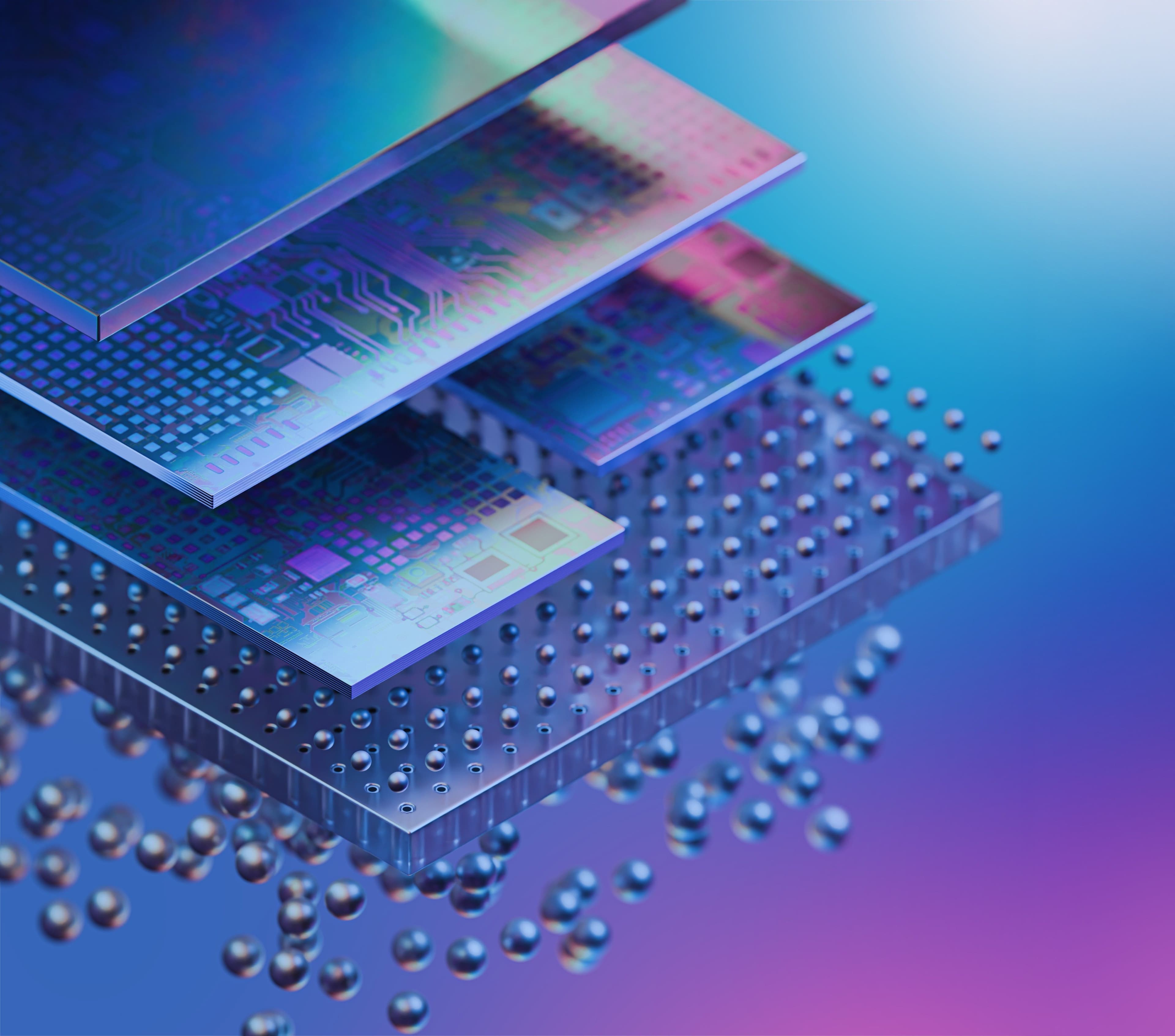
LEUVEN (Belgium), May 12, 2026 — Imec, a world-leading research and innovation hub in advanced semiconductor technologies, announced that IC-Link by imec, imec’s design and manufacturing service provider for ASICs and silicon photonics, has joined the TSMC Open Innovation Platform® (OIP) 3DFabric® Alliance. As part of the TSMC OIP ecosystem, the 3DFabric Alliance enables 3D integrated circuit (IC) innovation, readiness and customer adoption of TSMC’s 3DFabric, a comprehensive family of 3D silicon stacking and advanced packaging technologies including TSMC-SoIC®, CoWoS®, InFO, and TSMC-SoW™. Through this partnership, IC-Link will enhance its capabilities in advanced chip integration, while customers and the expanded 3DFabric ecosystem will be able to leverage imec’s global ASIC services.
The continued growth of AI, high-performance computing, and memory-intensive applications push traditional chip design approaches to their limits. Increasingly, system performance, power efficiency, and cost are determined not only by transistor scaling, but by how multiple chip components are integrated into a cohesive system. Integration of multiple chip components and memory through advanced packaging has therefore moved from a backend consideration to a central element of chip innovation.
For ASICs this shift demands a new level of collaboration. Designing leading-edge silicon and packaging requires co-optimization through iterative development cycles between the design, integration, and manufacturing teams. Through TSMC’s 3DFabric Alliance, partners gain early access to 2.5D/3D technologies enabling accelerated solution development. This ultimately will give IC-Link's customers a headstart to develop 3D IC innovation solutions and stay at the cutting edge of ASICs.
“Building on imec’s deep expertise in advanced packaging and heterogeneous integration, IC-Link now joins the TSMC 3DFabric Alliance, sending a clear signal that it is ready to take on the industry’s most advanced projects, particularly in Europe and North America,” said Ozgur Gursoy, Director Portfolio & Strategy for IC-Link’s ASIC services. "The collaboration is especially relevant for companies designing semiconductors for HPC, automotive, mobile, and telecommunications markets, where advanced packaging has become a decisive factor in performance, power efficiency, and time-to-market. Through the 3DFabric Alliance, our customers gain access to advanced packaging know-how and a smoother path to high-volume manufacturing and industrialization and still benefit from our flexible business models.”
"The relentless pursuit of higher performance and greater power efficiency continues to drive innovation in advanced packaging and 3D integration. At TSMC, we actively collaborate with our 3DFabric Alliance members to accelerate design enablement through our transformative 3D IC technologies,” said Aveek Sarkar, Director of the Ecosystem and Alliance Management Division at TSMC. "We welcome imec's expanded collaboration with the OIP ecosystem through the 3DFabric Alliance and look forward to working together to bring even greater value to the industry."
IC-Link by imec has been a TSMC Value Chain Alliance (VCA) member since 2009 and Design Center Alliance (DCA) member since 2007 and is now a 3DFabric Alliance member headquartered in Europe, underlining its position as a global key player in advanced ASIC and system integration.
This expanded alliance reinforces imec’s strategic focus on system scaling and heterogeneous integration, connecting early-stage research directly with industrial implementation. As the industry moves toward modular, multi-die systems, partnerships like the TSMC OIP ecosystem and the 3DFabric Alliance will play a key role in enabling scalable, high-performance solutions for the next generation of computing.
About IC-Link by imec
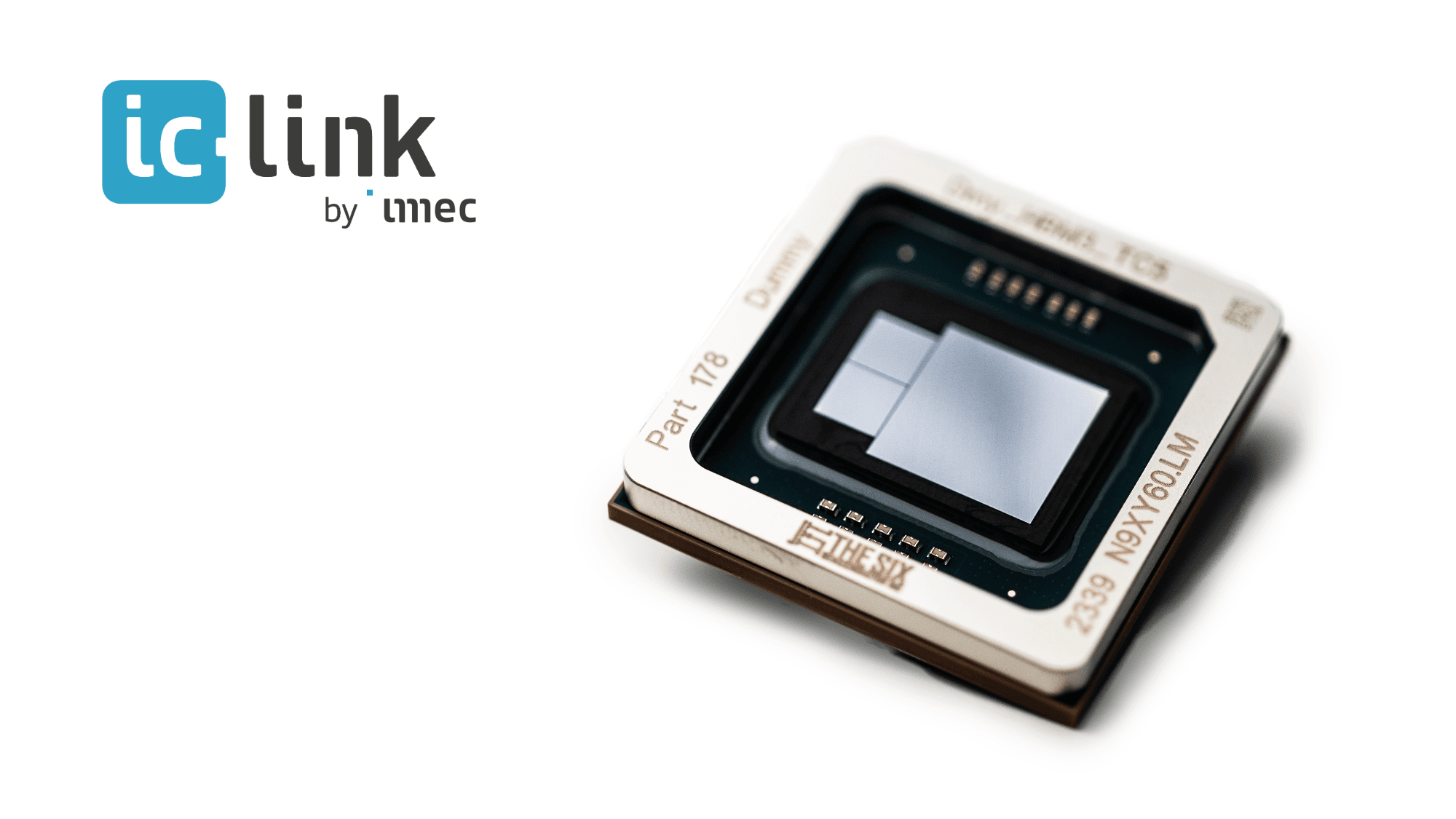
IC-Link by imec provides customized solutions for innovative chip manufacturing, leveraging the expertise and ecosystem of imec, a world-leading research and innovation center for nanoelectronics and digital technologies. IC-Link enables the scalable and reliable manufacturing of semiconductors to go from idea to product. Technologies range from ASICs in CMOS, including the most advanced commercially available nodes, to imec-developed integrated photonics, and advanced 2.5/3D packaging. Additional specialty services include custom wafer processing. The offering will continue to expand as new technologies are validated. To tailor to customer requirements and capabilities, IC-Link offers a range of services and business models.
For more information, visit www.imeciclink.com or www.imec-int.com
The imec group holds a global trademark portfolio, including word marks and combined figurative registered and unregistered trademarks, across national, regional, and international territories. Its lawful use requires prior written consent of IMEC in compliance with the IMEC branding guidelines, which may be updated periodically. The latest version is available upon written request.