Imec demonstrates die-to-wafer hybrid bonding with a Cu interconnect pad pitch of 2µm
Improved die-to-wafer assembly flow opens doors to logic/memory-on-logic stacking, and to optically interconnected systems-on-wafer
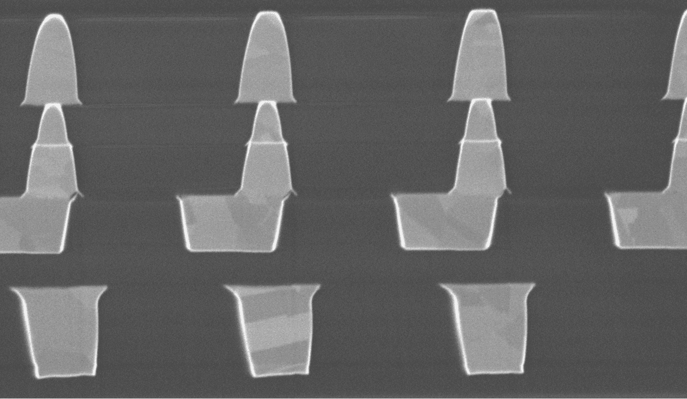
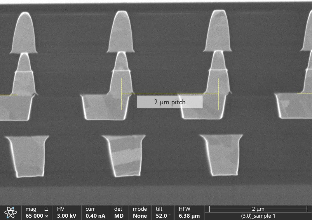
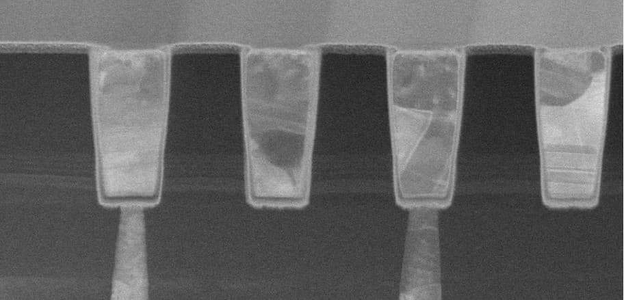
LEUVEN (Belgium), MAY 29, 2024— This week, at the 2024 IEEE Electronic Components and Technology Conference (ECTC), imec, a world-leading research and innovation hub in nanoelectronics and digital technologies, presents a Cu-to-Cu and SiCN-to-SiCN die-to-wafer bonding process resulting in a Cu bond pad pitch of only 2µm at <350nm die-to-wafer overlay error, achieving good electrical yield. Such fine-grained die-to-wafer interconnects pave the way to logic/memory-on-logic and memory-on-memory applications. On the longer term, die-to-wafer bonding will enable also die- and wafer-level optical interconnects – for which imec demonstrated a first proof of concept at ECTC2024.
Imec is developing a process flow for direct die-to-wafer hybrid bonding at interconnect pad pitches well below 10µm, down to 1µm. To reach these goals, imec achieved a major process improvement, in particular preserving ultraclean surfaces during processing, die singulation and pick-and-place; and maintaining a high throughput during all the process steps. This has led to a first demonstration with a Cu bond pad pitch scaling down to 2µm.
Hybrid bonding requires very high-quality surface preparation to achieve smooth surfaces with minimal Cu pad recess (<2.5nm), requiring careful optimization of the chemical-mechanical polishing (CMP) step of the Cu/SiCN surface. These properties need to be maintained during wafer singulation and die-to-wafer placement. To achieve a high-quality die singulation, without particles and impact to the Cu/SiCN surface, a plasma dicing process was implemented. Critical to the pad pitch scaling is a fast but high accuracy pick-and-place step. The die processing together with a high-accuracy pick-and-place step resulted in <350nm die-to-wafer overlay errors. The assembly flow enabled 2µm pitch Cu bond pads with good electrical yield: Kelvin e-yield >85% and daisy chain e-yield >70%.
Eric Beyne, senior fellow, VP of R&D, and program director 3D system integration at imec: “In terms of interconnect pitch, die-to-wafer hybrid bonding can now bridge the gap between solder-based die-to-wafer bonding (which is likely to stagnate at 10 to 5µm bump pitch) and wafer-to-wafer hybrid bonding (allowing interconnects well below 1µm, down to 400nm pitch (as presented at IEDM 2023), and possibly 200nm pitch in the future). Compared to the latter, die-to-wafer bonding offers the advantage of stacking only known-good dies (resulting in higher compound yields) and of bonding dies of unequal size. Future improvements to our process flow will further push the interconnect pitch towards 1µm. With this evolution, die-to-wafer bonding can enter the realm of memory/logic-on-logic and memory-on-memory stacking.”
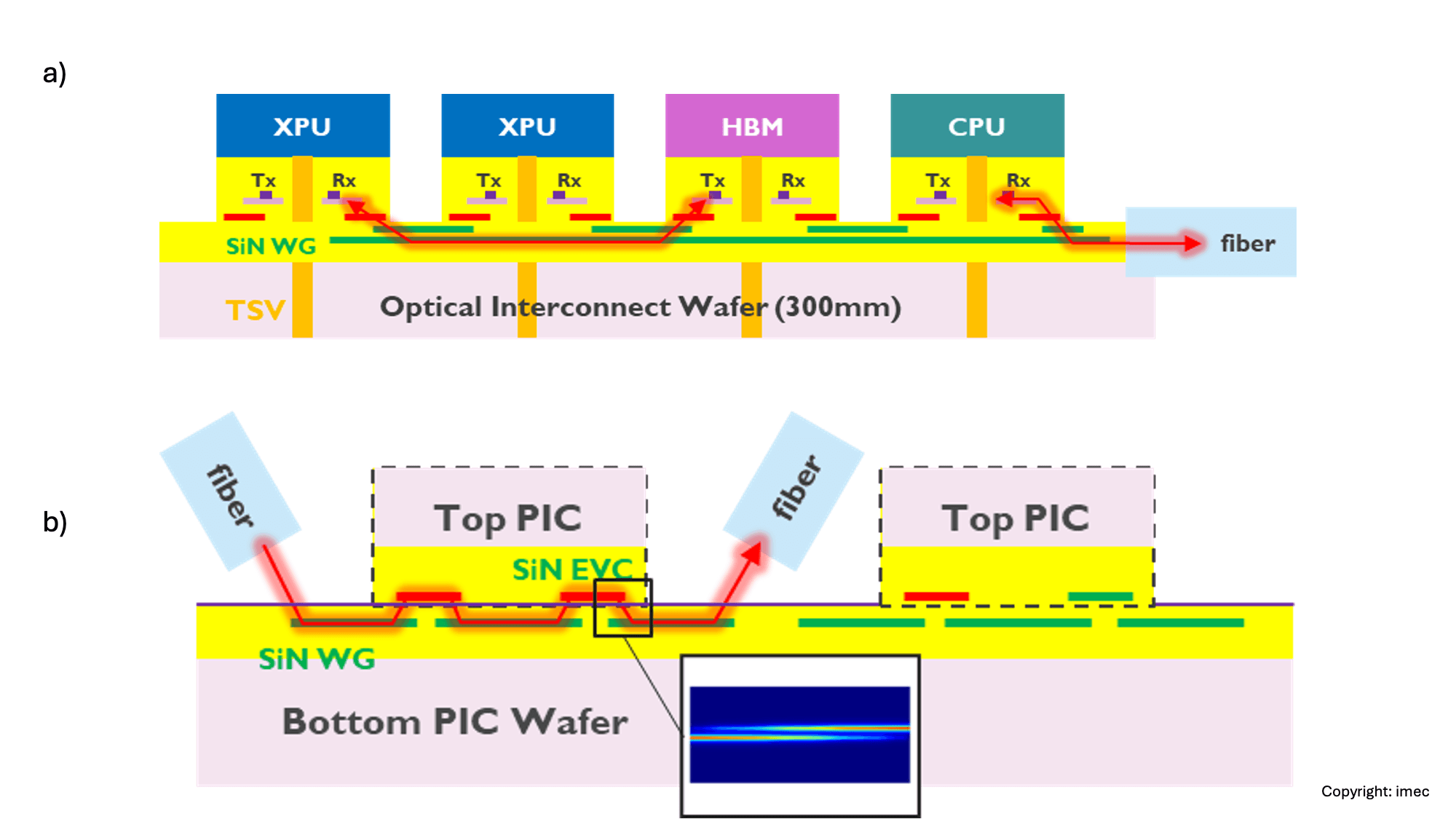
In addition, high-precision die-to-wafer bonding processes are a key enabler for wafer-level optical interconnects – imec’s long-term vision for high-bandwidth, low-power connections between multiple compute chips (xPUs) and high-bandwidth memory (HBM) in AI/ML clusters. An attractive approach from cost and yield perspective is to partition the optical interconnect in a passive optical interconnect wafer, containing long-range routing waveguides and passive optical functions, and active photonic IC (PIC) dies (with modulators and photodetectors) – which in turn are bonded to an electrical IC (XPU or HBM). Joris Van Campenhout, fellow and R&D program director at imec: “As a first proof of concept, we enabled low-loss evanescent optical coupling between PIC dies and a 300mm bottom optical interconnect wafer – leveraging a (collective) SiCN dielectric-based die-to-wafer assembly process. Benefitting from the accurate die-to-wafer alignment, low optical coupling losses of below 0.5dB were obtained. In the next steps, we will expand our assembly flow – e.g. by also providing Cu-to-Cu interconnects throughout the die-to-wafer stack.”
An overview of other imec contributions at ECTC 2024, can be found here.
About imec
Imec is a world-leading research and innovation center in nanoelectronics and digital technologies. Imec leverages its state-of-the-art R&D infrastructure and its team of more than 5,500 employees and top researchers, for R&D in advanced semiconductor and system scaling, silicon photonics, artificial intelligence, beyond 5G communications and sensing technologies, and in application domains such as health and life sciences, mobility, industry 4.0, agrofood, smart cities, sustainable energy, education, … Imec unites world-industry leaders across the semiconductor value chain, Flanders-based and international tech, pharma, medical and ICT companies, start-ups, and academia and knowledge centers. Imec is headquartered in Leuven (Belgium), and has research sites across Belgium, in the Netherlands and the USA, and representation in 3 continents. In 2023, imec's revenue (P&L) totaled 941 million euro.
Further information on imec can be found at www.imec-int.com.
Imec is a registered trademark for the activities of imec International (IMEC International, a legal entity set up under Belgian law as a “stichting van openbaar nut”), imec Belgium (IMEC vzw supported by the Flemish Government), imec the Netherlands (Stichting IMEC Nederland supported by the Dutch Government), imec Taiwan (IMEC Taiwan Co.), imec India (IMEC India Private Limited), imec San Francisco (IMEC Inc.) and imec Florida (IMEC USA Nanoelectronics Design Center Inc.).
Discover more

Sony and imec unveil high-density backside connectivity module enabling next-generation 3D chip integration
Read more
ASML, TSMC and imec bring industry-ready 2D-material transistors closer with breakthrough 300mm integration
Read more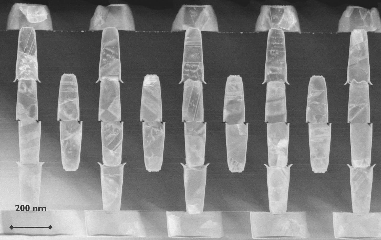
Imec and EV Group demonstrate wafer-to-wafer hybrid bonding with 200nm interconnect pitch and record high overlay accuracy
Read more