Chiplets: Piecing Together the Next Generation of Chips (Part II)
Testing the limits: standardization and optimization of chiplet test protocols

In short
Chiplets are small chips with a well-defined function that can be incorporated with other chiplets into a single package or system. They often come from different sources, making electrical testing challenging.
Here, we describe imec’s role in the standardization and optimization of 3D testing protocols.
This is the second part of a two-part series dedicated to chiplets, Part I was previously published here. The series addresses recent developments in interconnect technologies (part I) and testing strategies and standardization efforts (part II).
This article first appeared in 3DInCites. You can find it here.
Chiplets are here to stay
Chiplets are modular chips with a specific function that are separately fabricated and then interconnected to form a larger system. They have emerged as a promising approach to address challenges in scaling of integrated circuits and offer versatility, scalability, and performance advantages over traditional, monolithic System-on-Chip (SoC) designs. Chiplet technology is relatively new. Just a handful of large semiconductor companies, such as AMD and Intel, have products on the market, while foundry TSMC is currently looking into standardizing the process of developing and combining chiplets on a substrate. Nevertheless, the global chiplet market is expected to grow at an annual rate of over 42% says a new report.
Electrical testing of chiplets ensures the reliability, functionality, and interoperability of these heterogeneous architectures. This article focuses on recent advancements in chiplet testing protocols and initialization of testing standards that extend beyond competitive boundaries.
Reliability and quality criteria
The quality of a chiplet refers to its condition at the moment of manufacturing. Chiplets -just like monolithic SoCs- follow certain quality criteria per application field in the manufacturing process, covering aspects such as performance and functionality. Despite rigorous testing, some defects remain undetected and ‘escape’ to the final chiplet – the so-called ‘test escapes,’ A typical number of tolerated defects for consumer electronics such as mobile phones is 100dppm (defective parts per million). This means that for every million chiplets, 100 faulty ones are tolerated. Conversely, automotive is the most stringent application field, with customers asking for “0dppm” (which in reality translates to single-digit dppm). That is because electronics in a car are often critical for safety: if your airbag opens without a good reason due to a test escape, chances are high that the driver will cause an accident. And, even for seemingly trivial issues with the car radio, the end customer will not accept a new car if the radio does not play. Other demanding application fields are avionics and medical.
Chiplets are tested after production to identify potential failure mechanisms during their operational lifetime, including heating, cooling down, or thermo-shock vibration testing to ensure reliability.
Design-for-Test standard
Because chiplet-based integrated circuits are assembled from discrete components, they typically feature more potential test moments than monolithic SoCs fabricated as an integrated system. For example, pre-bond, the individual chiplets are checked to ensure they meet specifications and are free from defects. Afterward, the integrity and reliability of interconnects are tested. Finally, once the chiplets are assembled, the design as a whole is evaluated.
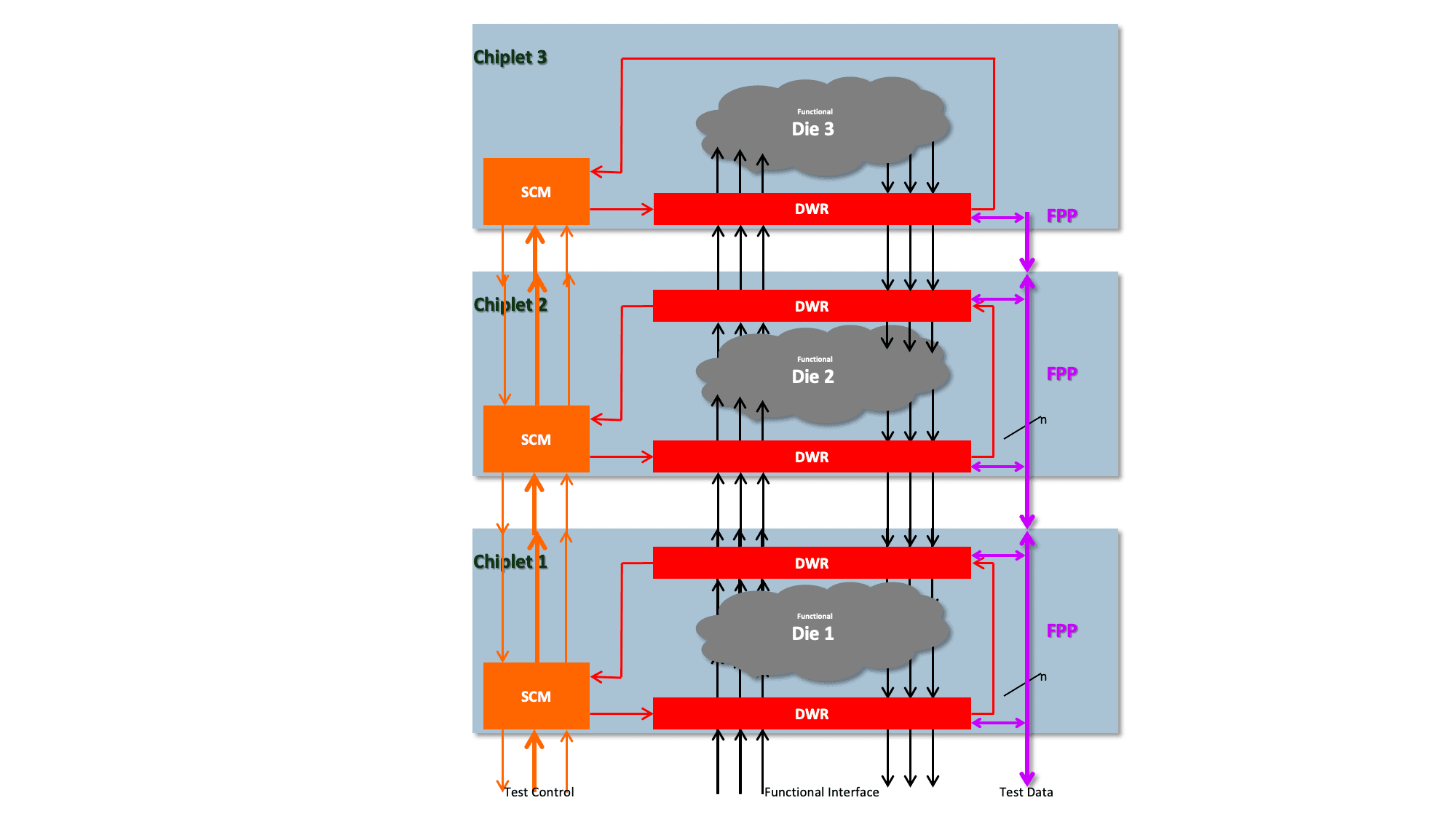
One of the major challenges in electrical testing of 2.5D and 3D chiplet-based designs is to reach every chiplet of the design with the test stimuli and read out the responses. To ensure chiplets from different sources have test access compatibility, imec initiated the standardization of IEEE Std 1838TM of 3D-DfT for test access.
For example, to test chiplet number three in a stack of four chiplets (one = bottom, four = top), chiplets number one and two require ‘design-for-test’ (DfT) structures to ensure the transport of test stimuli and test responses through those dies. Since chiplets can come from different vendors, these DfT structures must be standardized to ensure communication. Since 2020, IEEE Std 1838TM has prescribed the standard DfT followed by all software companies specialized in electronic design automation (EDA).
Improved testing of interconnects
Up to now, companies were used to developing their chips from A to Z with their own dedicated design flows and tools. However, in a chiplet-based approach, chiplets from different vendors must speak the same language to connect effectively. In other words, standardization is needed. The Universal Chiplet Interconnect Express (UCIe) is a standard focused on interconnections between dies or chiplets and reaches over the borders of competitive companies.
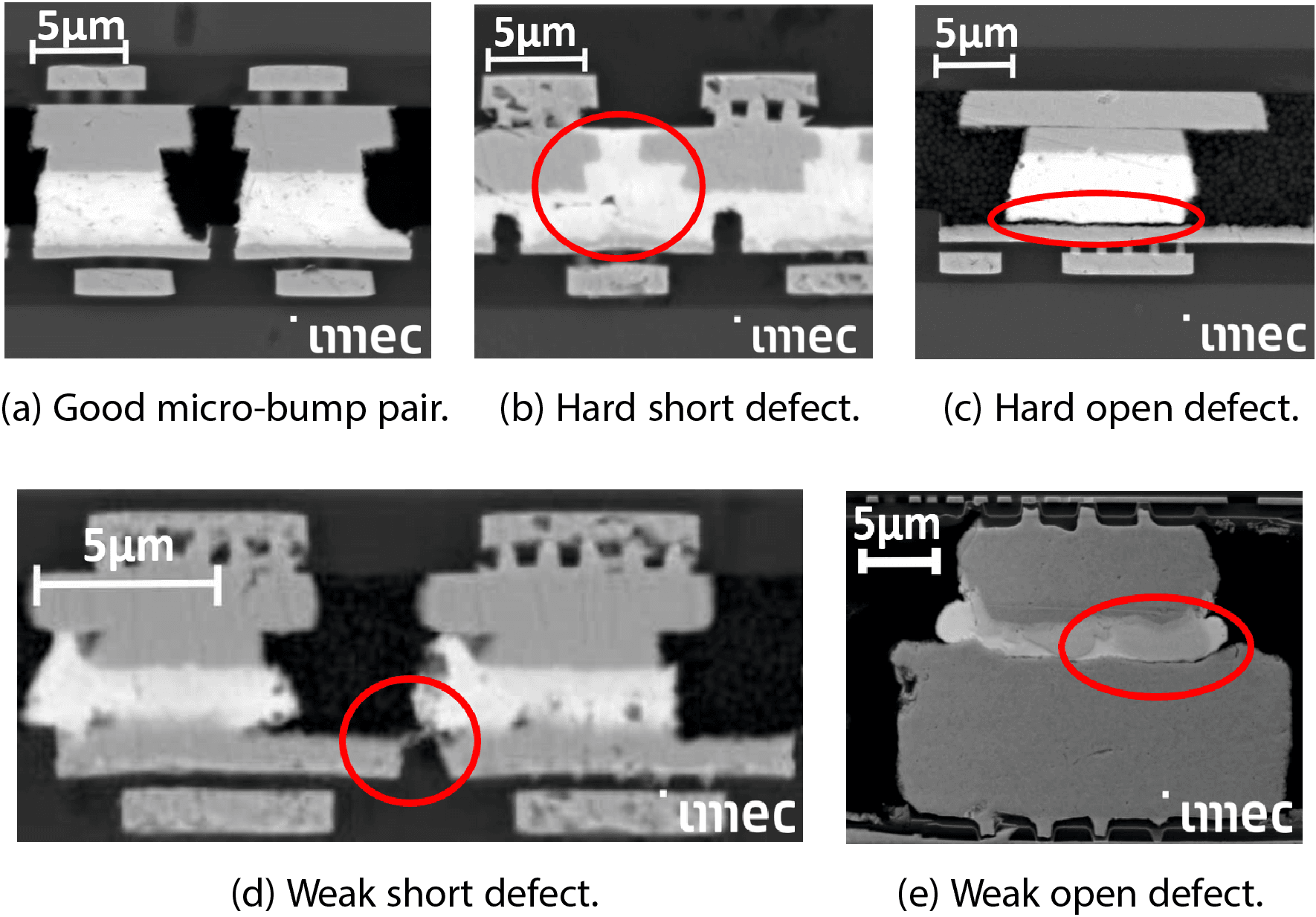
Current interconnect test methods target hard open and short defects, with a 2× ⌈log2(k)⌉ test pattern count for k interconnects. Recently, imec proposed an improved interconnect test generation method (E2I-TEST) that is more effective by also covering weak defect variants (high-resistive shorts and low-resistive open defects). It improves the test efficiency by considering only shorts between adjacent interconnects. As a bonus, it only requires 8 × ⌈log2(4)⌉ = 16 test patterns, thereby decoupling the test pattern count from the dependency on the number of interconnects k, which is large already today and only expected to grow.
Want to know more?
- This press release announces the publication of IEEE Std 1838 that imec initiated. Over the years, imec has also engaged in multiple joint development programs regarding testing with key players in the field, for example Cadence and Cascade Microtech.
- A recent article describes the improved interconnect test generation method and modifications to the UCIe specification: Chuang, P.-Y., Lorenzelli, F., & Marinissen, E. J. (2023). Generating Test Patterns for Chiplet Interconnects: Achieving Optimal Effectiveness and Efficiency. In: 2023 IEEE International Test Conference in Asia, ITC-Asia 2023. https://doi.org/10.1109/ITC-Asia58802.2023.10301169.
- Imec organized and spoke at a special session about “IEEE Std P3405: New Standard-under-Development for Chiplet Interconnect Test and Repair” at the IEEE VLSI Test Symposium (VTS 2024) and the IEEE European Test Symposium (ETS 2024).
- Also at ETS 2024:
- Imec presented the paper: Tsung-Hsuan Wang, Po-Yao Chuang, Francesco Lorenzelli, Erik Jan Marinissen. Test and Repair Improvements for UCIe.
- Imec organized a one-day fringe workshop, CITaR: 1st IEEE International Workshop on Chiplet Interconnect Test and Repair
Authors

Erik Jan Marinissen
Erik Jan Marinissen is Principal Scientist at imec, where he is responsible for research on test and design-for-test. In addition, he is Visiting Researcher at Eindhoven University of Technology, the Netherlands. Previously, he worked at NXP Semiconductors and Philips Research Laboratories in Eindhoven. Marinissen holds an MSc degree in Computing Science (1990) and a PDEng degree in Software Technology (1992), both from Eindhoven University of Technology. He is (co-)author of 280+ journal and conference papers and (co-)inventor on 15 granted US/EP patent families. Marinissen is IEEE Fellow and Golden Core member of Computer Society.

Eric Beyne
Eric Beyne obtained a degree in electrical engineering in 1983 and the Ph.D. in applied sciences in 1990, both from the Katholieke Universiteit Leuven, Belgium. Since 1986 he has been with imec in Leuven, Belgium where he has worked on advanced packaging and interconnect technologies. Currently, he is imec fellow and program director of imec’s 3D system integration program. He received the European Semi Award 2016 for contributions to the development of 3D technologies.