New standard allows stacked dies in 3D integrated circuits to connect with test equipment

27/01/2020
3D integration

An imec-initiated industry collaboration leads to publication of IEEE Std 1838TM for test access architectures for 3D integrated circuits (3D-ICs)
Close-up of a semiconductor wafer with repeated chip patterns in green, gray and orange
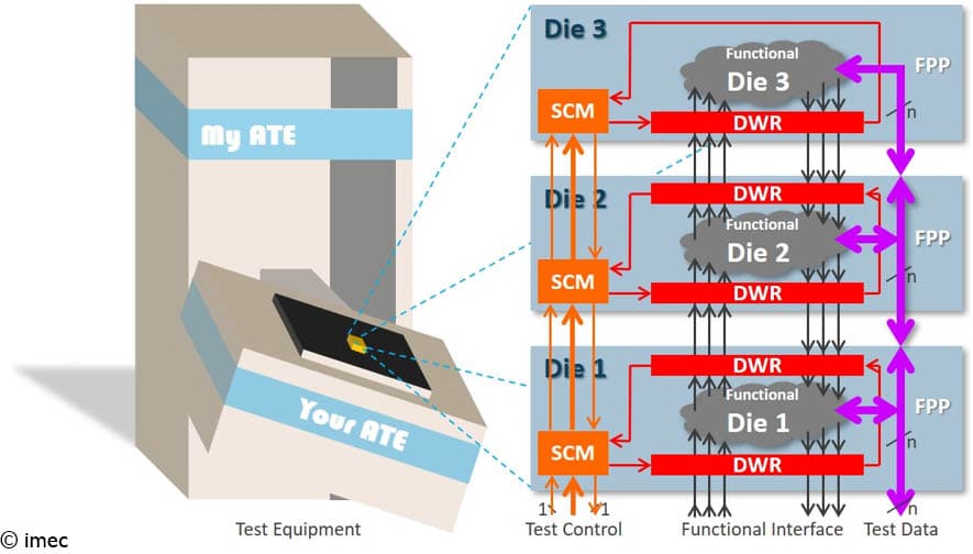
Diagram of test equipment connected to a 3D IC with three stacked dies and test access paths through each die.

About imec

Imec is a world-leading research and innovation hub in nanoelectronics and digital technologies. The combination of our widely acclaimed leadership in microchip technology and profound software and ICT expertise is what makes us unique. By leveraging our world-class infrastructure and local and global ecosystem of partners across a multitude of industries, we create groundbreaking innovation in application domains such as healthcare, smart cities and mobility, logistics and manufacturing, energy, and education.

As a trusted partner for companies, start-ups, and universities we bring together more than 4,000 brilliant minds from over 97 nationalities. Imec is headquartered in Leuven, Belgium and has distributed R&D groups at a number of Flemish universities, in the Netherlands, Taiwan, USA, and offices in China, India and Japan. In 2018, imec's revenue (P&L) totaled 583 million euro. Further information on imec can be found at www.imec-int.com.

Imec is a registered trademark for the activities of IMEC International (a legal entity set up under Belgian law as a "stichting van openbaar nut”), imec Belgium (IMEC vzw, supported by the Government of Flanders), imec the Netherlands (Stichting IMEC Nederland, part of Holst Centre which is supported by the Dutch Government), imec Taiwan (IMEC Taiwan Co.), imec China (IMEC Microelectronics (Shanghai) Co. Ltd.), imec India (Imec India Private Limited), and imec Florida (IMEC USA nanoelectronics design center).

Discover more
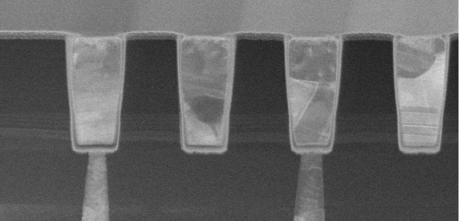
Scanning electron microscope view of hybrid-bonded interconnects with a 200 nm scale bar

Imec and EV Group demonstrate wafer-to-wafer hybrid bonding with 200nm interconnect pitch and record high overlay accuracy

28/05/2026
press release
3D integration
Read more
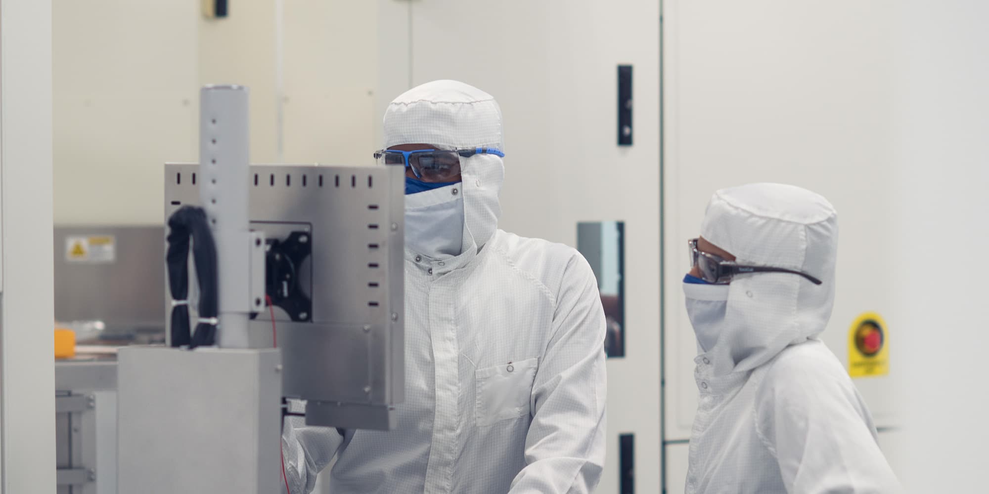
Two cleanroom technicians inspect semiconductor equipment in a white lab

3D integration

Page
3D integration
Read more
Illustration of stacked semiconductor chips and floating solder balls for 3D packaging

IC-Link by imec joins TSMC 3DFabric® Alliance to accelerate advanced packaging and 3D IC innovation

12/05/2026
press release
3D integration
Read more
Cross-section of wafer interconnects linking the front and backside

A path to high-density front- and backside wafer connectivity

19/08/2025
Page-turner
3D integration
CMOS: advanced & beyond
Read more
Two men standing in a modern corridor, likely company founders or executives

Vertical Compute, a new imec spin-off, raises €20 million to Revolutionize the Future of AI Computing

14/01/2025
press release
Venturing
3D integration
Read more
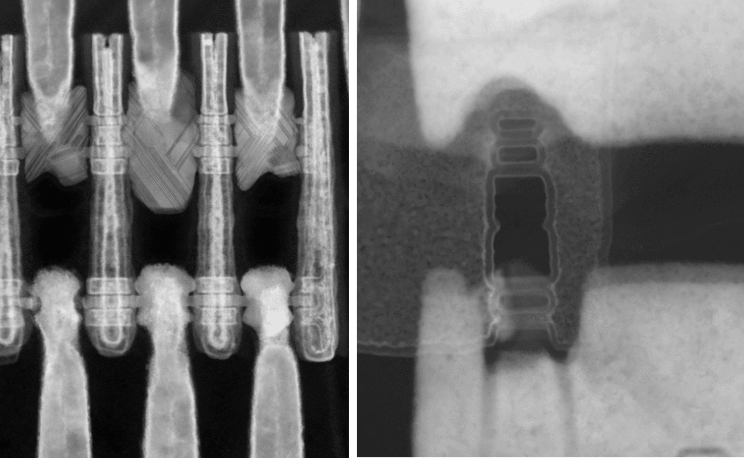
Microscope close-up of stacked transistor structures in a CFET device cross-section

Towards efficient ESD protection strategies for advanced 3D systems-on-chip

26/07/2024
Longread
3D integration
Read more
Glowing puzzle-piece chip on a circuit board, symbolizing chiplets and chip integration

Chiplets: Piecing Together the Next Generation of Chips (Part I)

16/07/2024
Longread
3D integration
Automotive
Read more
Groene lichtpuntjes verspreid over horizontale lagen, als een abstract beeld van vloeistofgeheugen

CMOS 2.0: bringing heterogeneity inside the system-on-chip

01/07/2024
Vision
CMOS: advanced & beyond
3D integration
Read more
SEM close-up of copper interconnect pads for die-to-wafer hybrid bonding

Imec demonstrates die-to-wafer hybrid bonding with a Cu interconnect pad pitch of 2µm

29/05/2024
press release
CMOS: advanced & beyond
3D integration
Read more

imec in your region

Looking for information about imec's activities in different parts of the world?

United Kingdom
United States
Qatar