Logic technology scaling options for 2nm and beyond
A roadmap marked by increased synergy between advanced logic device and nano-interconnect research

In short
In this interview, Naoto Horiguchi, director CMOS device technology, and Zsolt Tokei, imec fellow and program director nano-interconnects at imec, offer the semiconductor industry a broad spectrum of options to scale logic technology generations beyond 1nm.
Along the scaling path, they show how logic device development needs to go hand in hand with introducing innovations in the back-end-of-line, and, to an increasing extent, in the middle-of-line.
How do you see the scaling of logic devices evolving in the coming years?
Naoto Horiguchi: “A majority of IDMs and foundries have recently announced the transition from mainstream FinFET to gate-all-around (GAA) nanosheet FET architectures for their 3nm or 2nm logic technology generations. The forksheet architecture, which is an imec invention, could prolong this nanosheet generation. After the forksheet, we are anticipating complementary FETs (CFETs) to enter the logic scaling roadmap.”
“These transitions will allow us to gradually push track height scaling of standard cells below 4T, while still providing a power-performance advantage.
Beyond CFETs, 2D monolayer crystalline materials like tungsten disulfide (WS2) are promising replacements for Si in CMOS channels, offering opportunities for further gate-length scaling.”
How will these innovations impact the back-end-of-line? Which developments will be needed in the back-end- and middle-of-line to keep pace with scaling in the front-end-of-line?
Zsolt Tokei: “Advanced scaling in the front-end-of-line (FEOL) needs to go hand in hand with innovations in the back-end-of-line (BEOL) – the network of interconnects that needs to connect seamlessly to the underlying device structure. With the forksheet architecture entering the roadmap and cell heights being pushed below 5T, metal pitches in the critical BEOL layers will become as small as 20nm and below. This is extremely challenging from capacitance, resistance (via and wire) as well as from cost, printability and reliability point of view – requiring innovations at design, module and material level. This has driven the development of new interconnect integration schemes such as hybrid via metallization (addressing via resistance increase) and semi-damascene process flows – as a replacement for today’s mainstream Cu dual-damascene processes. Semi-damascene involves the direct etch of metal to achieve higher aspect ratio lines, and can include gapfill, partial or full air gaps to counter the capacitance increase.”
Naoto Horiguchi: “To strengthen the synergy between advanced logic device scaling and interconnect development, the middle-of-line (MOL) activities begin to play an increasingly important role. The MOL, which ties together the BEOL and the FEOL, has for a long time been organized as a single-layer contact to source, drain and gate.
But the transition to below-5T cell architectures drives the evolution towards multilayer MOL structures, in which extra layers and vias are added – similar to how the BEOL has evolved in the past.”
Which breakthrough did your team recently achieve?
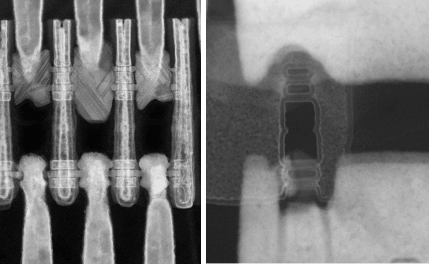
Naoto Horiguchi: “While the area and performance benefit of the forksheet device architecture was already shown through TCAD simulations, we have now for the first time presented electrical characterization of functional integrated forksheet FET devices – a breakthrough result that will be highlighted at the 2021 VLSI Symposium [1]. We have demonstrated the key modules of this architecture, including the dielectric wall and replacement metal gate patterning at 17nm n-p spacing. And although the forksheet device is a tri-gated device architecture, no degradation of the electrostatics has been observed in our work.”
Which avenues is imec exploring to complement this achievement from a nano-interconnect perspective?
Zsolt Tokei: “Extended nanosheet architectures such as the forksheet require new BEOL integration schemes such as semi-damascene to enable sub-20nm metal pitches. At the same time, we are developing new multilayer MOL routing schemes, such as the vertical-horizontal-vertical (VHV) scheme. In combination with scaling boosters (such as self-aligned contacts and buried power rail (BPR)), these multilayer MOL schemes will pave the way to a more efficient intra-cell routing at smaller cell heights.”
Naoto Horiguchi: “Implementing the multilayer process flow in the MOL, in combination with scaling boosters such as the buried power rail (BPR) will largely enhance the scalability of our forksheet-based cell designs, pushing track heights from 5T to 4T. As such, introducing semi-damascene in the MOL is another example of the benefits brought about by the cross-fertilization between FEOL, MOL and BEOL activities.”
What are the next important milestones you expect to achieve?
Naoto Horiguchi: “Our program focus will move from forksheet to CFET gradually after forksheet key modules and device demonstration. The CFET architecture is complex due to its many degrees of freedom. Imec will quantify the power-performance-area (PPA) benefits and the complexity of CFET process flows and recommend best option(s) to our partners. While nanosheet, forksheet and CFET architectures will gradually reduce cell track heights to 4T and beyond, we are exploring alternative device architectures that might address the slowdown in scaling the contact poly-pitch (CPP), which measures from one transistor’s gate contact to the gate contact on the adjacent device.”
Zsolt Tokei: “Evolution towards the 1nm CFET family of logic devices drives the development of new BEOL and MOL solutions. In the BEOL, we earlier proposed a new metallization construct referred to as ‘hybrid height with zero via’. In this construct, each metal layer is now split into three separate sub-layers, which allows to tune the height and aspect ratio of the metal lines (and hence, exchange resistance for capacitance) depending on their application need.
We are excited to report on a first SRAM assessment, confirming a significant improvement in read speed (by 30%) and write margin (by 50%). Currently, we are working towards real logic cell layouts.”
“On the longer term, we will need to complement these integration schemes with the introduction of new conductors. Of interest are ordered binary or ternary compounds with better figure of merit than e.g. Ru or Mo. We have already been pioneering this field with first ab initio simulations and initial experiments, and we are now intensifying our activities in close collaboration with imec’s materials R&D group.”
What is the key message you want the chip industry to remember?
Naoto Horiguchi: “In recent years, several people have claimed that traditional CMOS scaling has already come to an end. But with many innovations in the pipeline, we are convinced that we can continue CMOS scaling for at least the next ten years. Imec is a good place to work towards that goal. The close collaboration with our partners helps us to address the industry’s biggest challenges and push logic device scaling beyond the 1nm technology generation – leveraging the tight collaboration with imec’s nano-interconnect, Insite and material development activities.”
Zsolt Tokei: “Also from a BEOL perspective, we have many interesting and valid options allowing us to address the RC delay bottleneck and to pipeline interconnects for the coming ten years. We can offer our partners a comprehensive roadmap with a broad spectrum of options that are relevant for future logic device scaling, and of which the elements can be re-used for memory development. We are continuously enriching this roadmap with new insights, improved integration schemes and new materials – some of which will be also presented at the upcoming IITC conference in July.”
Want to know more?
[1] To learn more about imec’s presence at the 2021 VLSI Symposia, check out our program.
Authors

Naoto Horiguchi
Naoto Horiguchi is a director of the logic CMOS scaling program in imec, Leuven, Belgium. He started his carrier in semiconductor device R&D in Fujitsu Laboratories Ltd. in 1992. In 1992-1999, he was engaged in device development by using semiconductor nanostructures in Fujitsu laboratories Ltd. and University of California, Santa Barbara. In 2000 to 2006, he was engaged in 90-45nm CMOS technology development in Fujitsu Ltd. as a lead integration engineer. From 2006, he is with imec, Leuven, Belgium, where he is engaged in advanced CMOS device R&D together with worldwide industrial partners, universities and research institutes. His current focus is CMOS device scaling down to 2nm technology node and beyond.

Zsolt Tokei
Zsolt Tokei is Distinguished Member of Technical Staff Interconnects at imec. He joined imec in 1999 and since then held various technical positions in the organization. First as a process engineer and researcher in the field of copper low-k interconnects, then he headed the metal section. Later he became principal scientist, Program Director Nano-Interconnects and, in 2016, was appointed Distinguished Member of Technical Staff Interconnect. He earned a M.S. (1994) in physics from the University Kossuth in Debrecen, Hungary. In the framework of a co-directed thesis between the Hungarian University Kossuth and the French University Aix Marseille-III, he obtained his PhD (1997) in physics and materials science. From 1998 he worked at the Max-Planck Institute of Düsseldorf, Germany, as a post-doctorate researcher. From the date of joining imec he continued working on a range of interconnect issues including scaling, metallization, electrical characterization, module integration, reliability and system aspects.
Discover more