Imec demonstrates functional monolithic CFET devices with stacked bottom and top contacts
LEUVEN (Belgium), JUNE 18, 2024— This week, at the 2024 IEEE Symposium on VLSI Technology & Circuits (2024 VLSI), imec, a world-leading research and innovation hub in nanoelectronics and digital technologies, presents for the first time electrically functional CMOS CFET devices with stacked bottom and top source/drain contacts. While the results were obtained with both contacts patterned from the frontside, imec also shows the feasibility of moving bottom contact formation to the wafer backside – significantly improving top device survival rate from 11% to 79%.
Imec’s logic technology roadmap envisions the introduction of complementary FETs (CFETs) in A7 node device architectures. When complemented with advanced routing techniques, CFETs promise to reduce standard cell track heights from 5T to 4T and even below, without performance degradation. Among the different approaches to integrate n- and pMOS vertically stacked structures, monolithic integration is considered the least disruptive compared to existing nanosheet-type process flows.
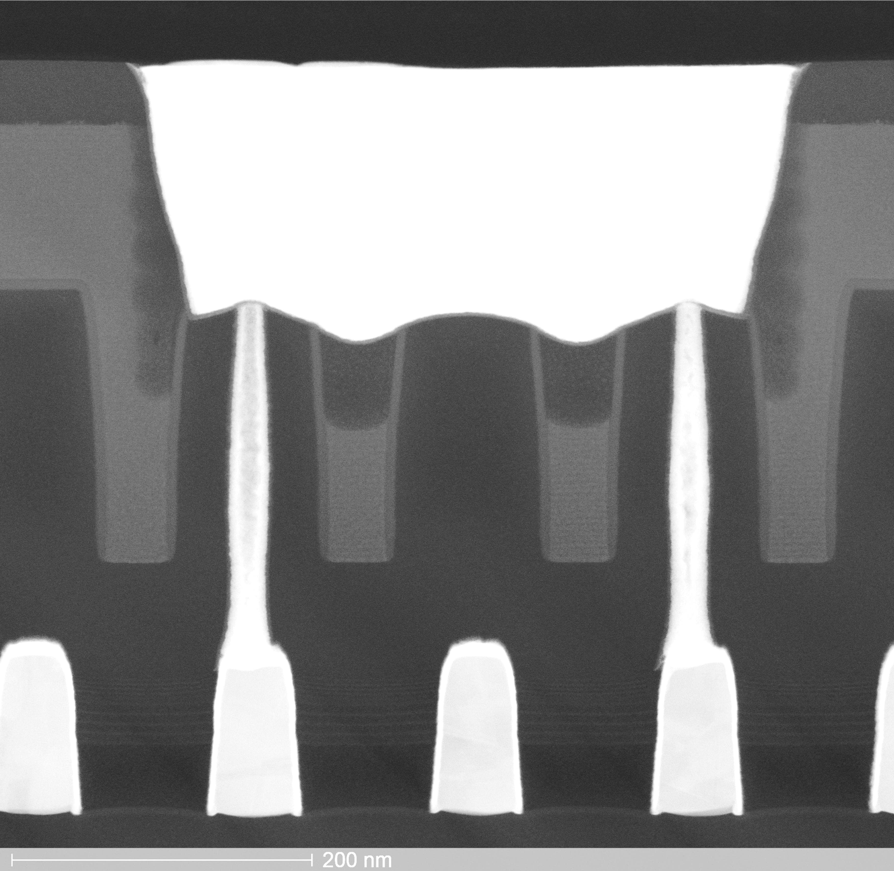
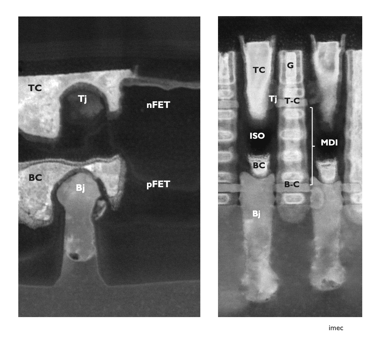
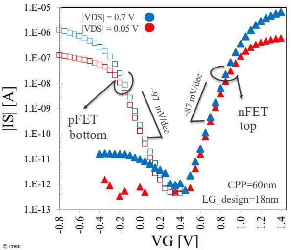
At the 2024 VLSI Symposium, imec demonstrates for the first time functional monolithic CMOS CFET devices with stacked top and bottom contacts. The CFETs were integrated at 18nm gate length, 60nm gate pitch and 50nm vertical separation between n and p devices. Electrical functionality was demonstrated on a test vehicle with nFET and pFET devices using a common gate, and top and bottom contacts connected from the frontside.
The proposed process flow includes two CFET-specific modules: the middle-dielectric isolation (MDI), and the stacked bottom and top contacts.
MDI is a module pioneered by imec to isolate top and bottom gate and differentiate on the threshold voltage settings between n and p devices. The MDI module is based on modifying the CFET ‘active’ multi-layer Si/SiGe stack and allows the co-integration of the inner spacer – a nanosheet-specific feature that isolates the gate from the source/drain. Naoto Horiguchi, Director CMOS device technology at imec: “We obtained the best results in terms of process control with an MDI-first approach, i.e., before source/drain recess – the step where nanosheets and MDI are ‘cleaved’ to gain access to the channel sidewalls and start source/drain epi. An innovative source/drain recess etch with ‘in-situ capping’ enables MDI-first by protecting the gate hardmask/gate spacer during the source/drain recess.”
A second critical module is the formation of stacked source/drain bottom and top contacts, vertically separated by dielectric isolation. Key steps are the bottom contact metal fill and etch back, and subsequent dielectric fill and etch back – all within the same tight space as available for the MDI stack.
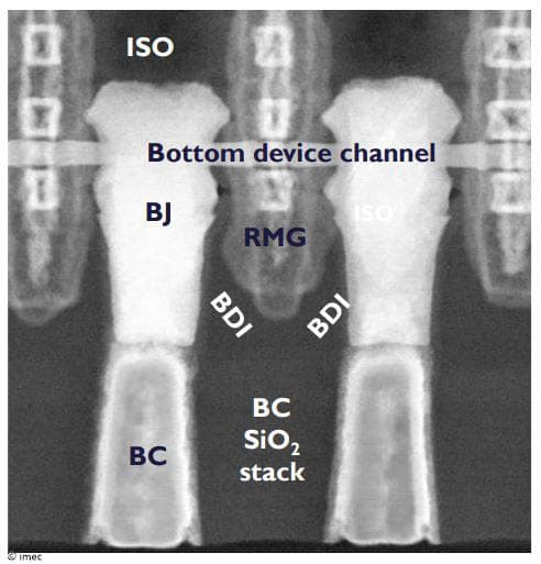
Naoto Horiguchi: “When developing the bottom contacts from the frontside, we encountered multiple challenges, affecting bottom contact resistance and limiting the process window for top device source/drain formation. At 2024 VLSI, we show that it is feasible to move the bottom contact formation to the wafer backside, despite additional process steps linked to wafer bonding and thinning. The top device survival rate increased from 11% to 79%, making backside bottom contact formation an attractive option for industry. Research is currently ongoing to identify the optimal contact routing approach.”
About imec
Imec is a world-leading research and innovation center in nanoelectronics and digital technologies. Imec leverages its state-of-the-art R&D infrastructure and its team of more than 5,500 employees and top researchers, for R&D in advanced semiconductor and system scaling, silicon photonics, artificial intelligence, beyond 5G communications and sensing technologies, and in application domains such as health and life sciences, mobility, industry 4.0, agrofood, smart cities, sustainable energy, education, … Imec unites world-industry leaders across the semiconductor value chain, Flanders-based and international tech, pharma, medical and ICT companies, start-ups, and academia and knowledge centers. Imec is headquartered in Leuven (Belgium), and has research sites across Belgium, in the Netherlands and the USA, and representation in 3 continents. In 2023, imec's revenue (P&L) totaled 941 million euro.
Further information on imec can be found at www.imec-int.com.
Imec is a registered trademark for the activities of imec International (IMEC International, a legal entity set up under Belgian law as a “stichting van openbaar nut”), imec Belgium (IMEC vzw supported by the Flemish Government), imec the Netherlands (Stichting IMEC Nederland supported by the Dutch Government), imec Taiwan (IMEC Taiwan Co.), imec India (IMEC India Private Limited), imec San Francisco (IMEC Inc.) and imec Florida (IMEC USA Nanoelectronics Design Center Inc.).