Unlocking tomorrow's technology nodes: inside imec's N2 P-PDK workshop
Hands-on training grants academia and industry access to cutting-edge semiconductor technologies.

In short
Imec’s N2 P-PDK workshop explores advanced semiconductor design strategies.
Participants from industry and academia gain hands-on N2 design experience, using tools from Synopsis and Cadence.
Imec’s initiative supports global semiconductor innovation and is closely tied to the European Chips Act objectives.
Moore's law has been the driving force behind decades of innovation in the semiconductor industry. Nodes continue to shrink and N2 is now the bleeding-edge tech. However, as technology nodes get smaller, achieving further performance gains becomes increasingly difficult. Addressing this challenge requires not only the development of new technological enablers, but also ensuring that the entire ecosystem is equipped with the latest insights into requirements, bottlenecks and breakthroughs.
In response to these demands, imec is offering low-barrier access to advanced technologies, a commitment exemplified by the NanoIC pilot line launched as part of the European Chips Act. In this context, imec recently hosted a two-day training session focused on its Pathfinding Process Design Kit (P-PDK) for N2 technology. Co-organized by Europractice, this workshop was aimed at industry professionals and academia, providing hands-on training on advanced node design.
You can freely download the N2 design pathfinding PDKs. Click here for access.
Bringing industry professionals and academia up to speed on the digital design of N2 tech
The workshop was all about making imec’s Pathfinding Process Design Kit (P-PDK) for advanced logic technologies accessible to industry and academia. It provided participants with a collection of code and files, bringing them up to speed on the digital design of N2 technology.
One of the key concepts covered was system-technology co-optimization (STCO). For years, the industry focused on design-technology co-optimization (DTCO) to keep advancing – but as nodes get smaller, achieving performance gains becomes more challenging. So, what is needed today are strategies that consider the entire system. Think of backside power delivery network (BSPDN) approaches – to give just one example. These are the types of functionalities that are part of imec’s P-PDK library, allowing participants to assess – and experiment with – specific N2 design features.
A course with a threefold objective
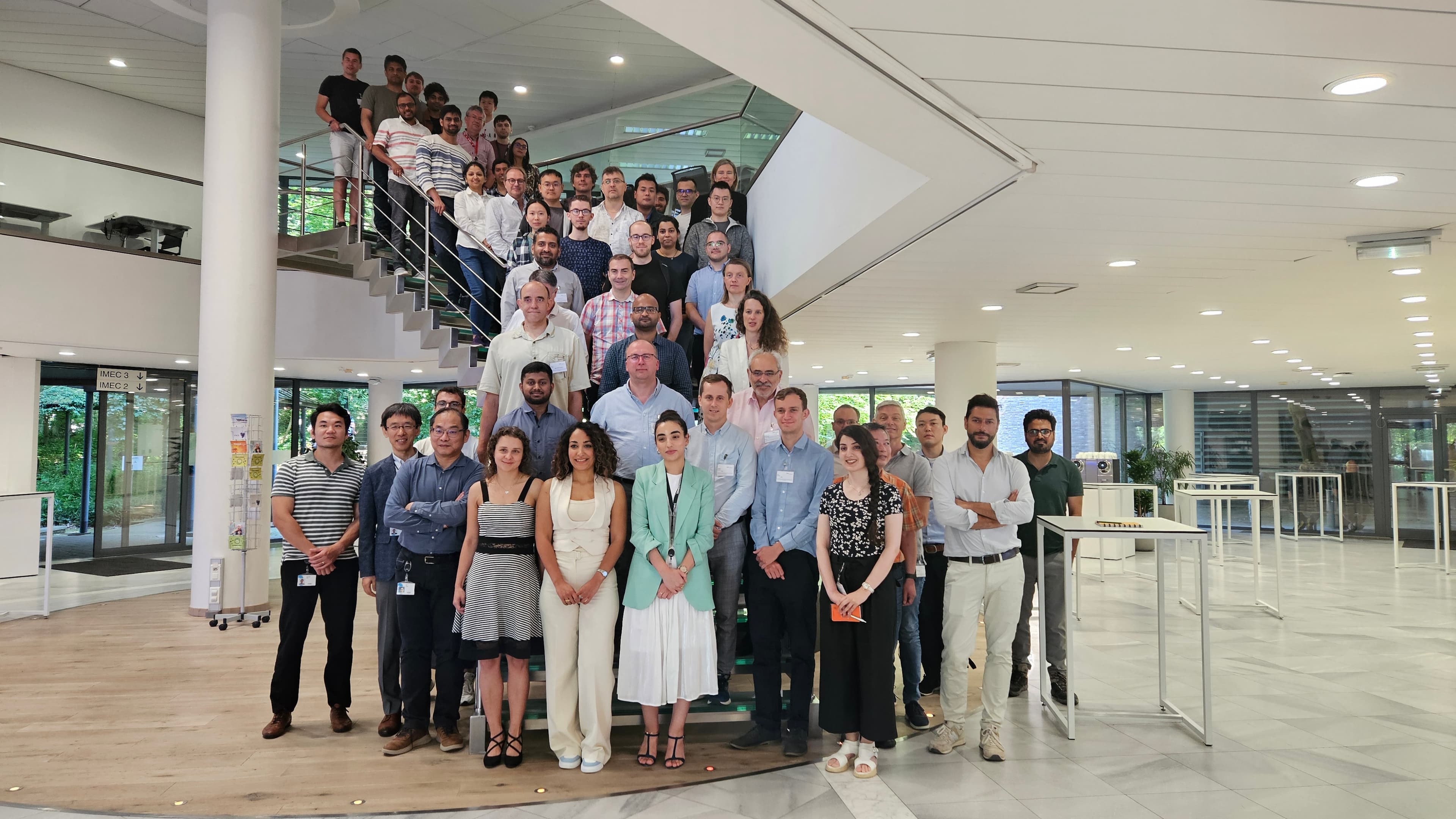
The workshop, spanning one and a half days, attracted great interest and participation. The first day consisted of a seminar providing a comprehensive overview of imec’s P-PDK, while the second half-day focused on hands-on training. Participants learned how to install the PDK and use electronic design automation (EDA) tools from Synopsis and Cadence, working through digital flows and exercises to gain a practical understanding of how different design strategies affect size and performance.
Sixty people attended the seminar on the first day and 25 were welcomed for the (fully-booked) hands-on training. Attendees included a mix of professionals from academia and industry, a turnout that underscores the strong demand for this type of initiative.
“By hosting this training and exploring opportunities for follow-up sessions, imec pursues a threefold objective. First, we aim to disseminate N2 technology to the design community and involve people in concepts like STCO at an early stage. Second, imec seeks to train participants in the specifics of advanced nodes, including new features such as BSPDN. Finally, we hope to motivate academic institutions to accelerate electronics research by exposing their members to the latest technological challenges and potential solutions.” - Anita Farokhnejad & Sara Louahdi, imec
Closely tied to the European Chips Act
Imec’s training session is not an isolated initiative. It is closely tied to the European Chips Act, which aims to propel research in advanced semiconductor nodes and develop a skilled workforce. Imec’s workshop accelerates these efforts by addressing an important gap: while academia still largely works with N14 technology, research centers like imec have already entered the Angstrom era. To achieve rapid progress, though, it is essential to bring the entire ecosystem up to speed on the latest technologies. Hence, imec’s workshop aims to create a win-win situation for all involved.
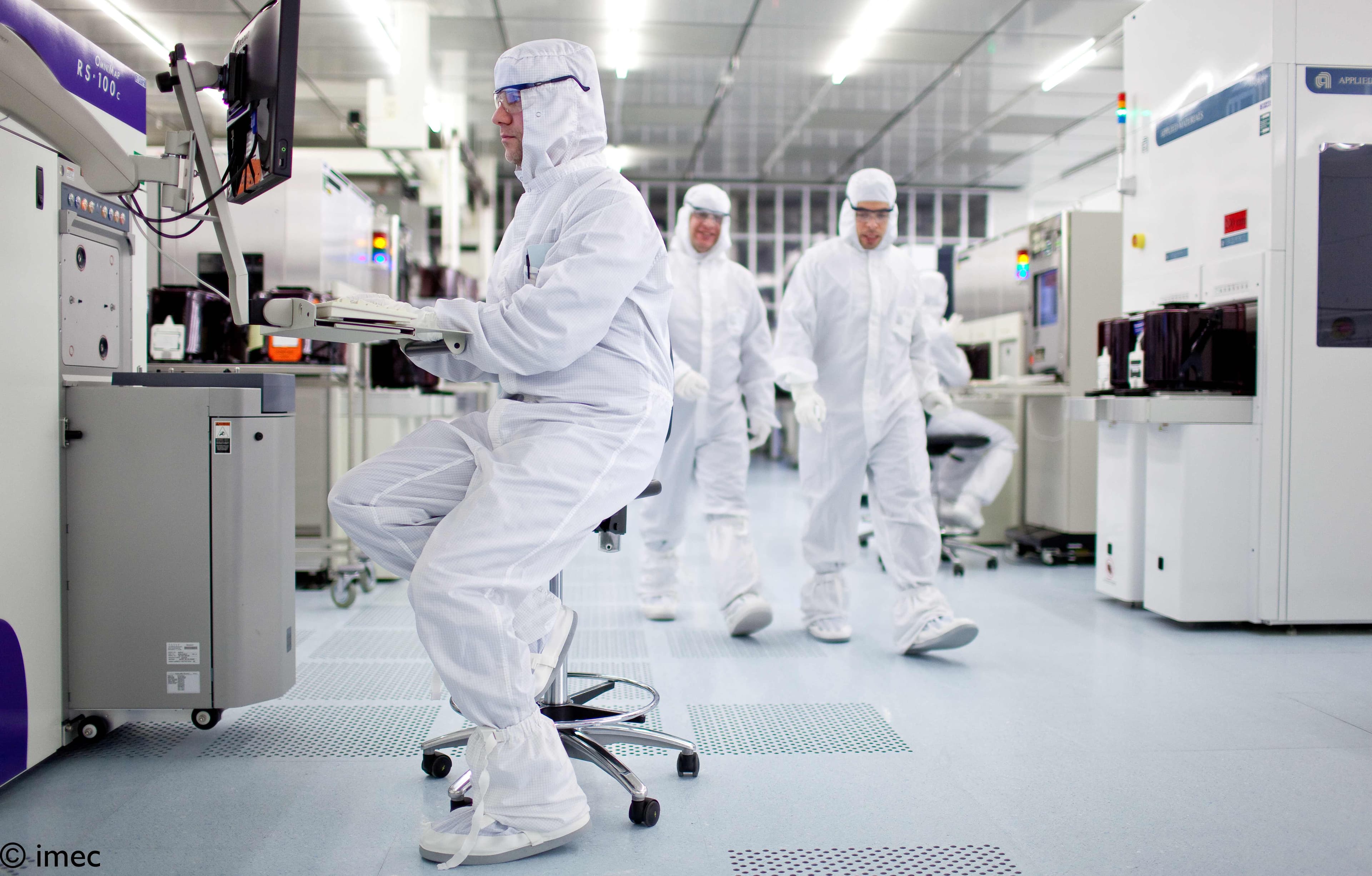
“Imec is a highly trusted, neutral contributor to semiconductor research worldwide. We provide infrastructure to – and share knowledge with – the entire ecosystem, leveraging a 12,000 square meter cleanroom, and the expertise of over 600 partners. This unique position allows us to share research findings at an early stage, something commercial companies cannot do without risking their competitive edge.” – Anita Farokhnejad & Sara Louahdi, imec
Want to stay informed about imec’s upcoming P-PDK workshops? Contact us atimecpdk@imec.be
Authors

Anita Farokhnejad
Anita Farokhnejad earned her PhD from Universitat Rovira i Virgili (Spain), specializing in FEOL and device modelling. She joined imec in 2021 as an R&D Engineer, focusing on BEOL optimization and future roadmap development. Collaborating closely with integration and physical design teams, she develops models for PnR data analysis and BEOL optimization. Her recent work on the enhanced Ring Oscillator (eRO) model aids in the early assessment of new materials and BEOL boosters. In August 2023, she advanced to team lead for PDK Enablement, translating advanced semiconductor nodes into Pathfinding-PDKs. Anita is also dedicated to education, conducting courses that make sophisticated technological concepts accessible to both industry veterans and aspiring engineers. Currently, she serves as Program Manager of DTCO at imec, where her contributions continue to drive innovation in the semiconductor industry.
Discover more