Imec demonstrates core building blocks of a scalable, CMOS-fab compatible superconducting digital technology
Record-performing NbTiN-based interconnects, Josephson junctions, and MIM capacitors open doors to energy-efficient compute systems for AI and HPC.
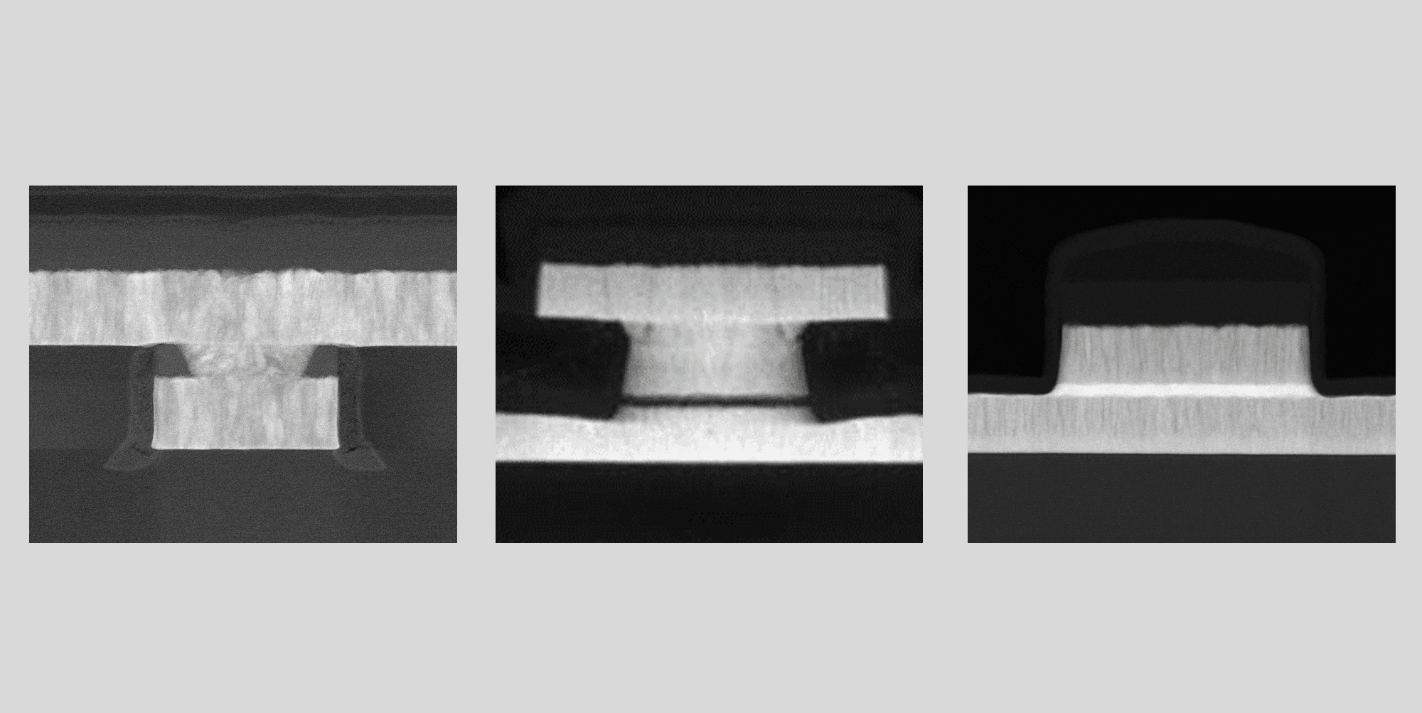
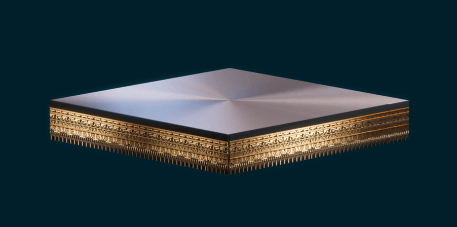
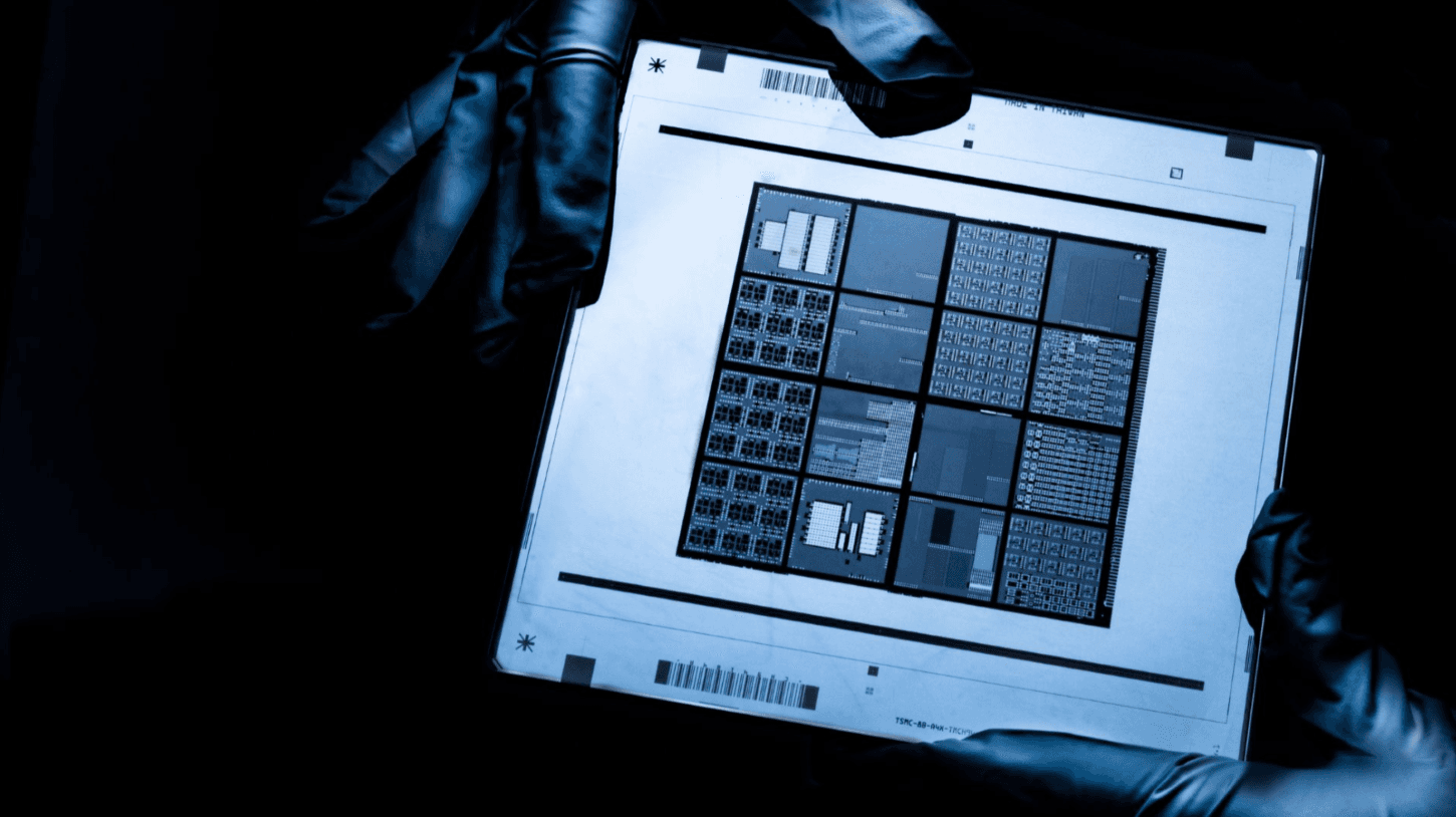
LEUVEN (Belgium) and Kissimee, FL (USA) December 10, 2024—This week, at the 2024 IEEE International Electron Devices Meeting (IEDM), imec, a world-leading research and innovation hub in nanoelectronics and digital technologies, demonstrates the three critical building blocks of a superconducting digital circuit: NbTiN-based interconnects, Josephson junctions, and MIM capacitors. The devices outperform state-of-the-art superconducting technology and meet the target specifications for superconducting digital systems designed to revolutionize the roadmaps for AI and HPC. Being scalable and compatible with CMOS fabrication technology, the demonstrated technology bridges the gap from lab-scale feasibility studies to industrial fabrication.
Compute systems based on superconducting digital technology promise to significantly outperform state-of-the-art CMOS-based processors by taking advantage of the zero electrical resistance of the superconducting materials at cryogenic temperatures. Imec, through a system-technology co-optimization study, showed that first-generation superconducting digital systems deliver 100x more system power efficiency and 10-100x better performance than a 7nm-CMOS-based system. To meet these target system specifications, a scalable technology is needed to fabricate the key building blocks of such superconducting digital circuits: superconducting interconnects (wires and vias), Josephson junctions serving as the active elements, and tunable MIM capacitors for power delivery.
Longread: superconducting digital technology to revolutionize the AI and machine learning roadmap
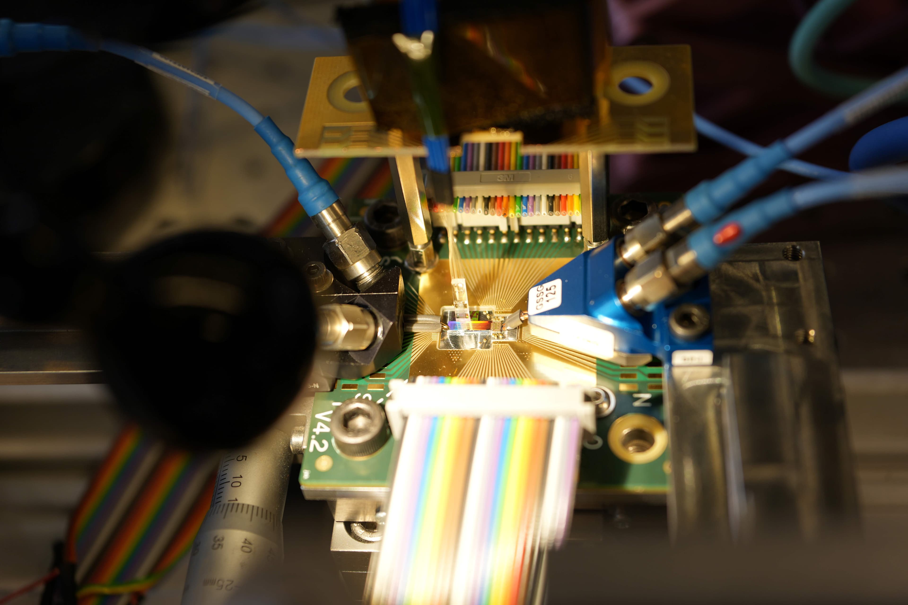
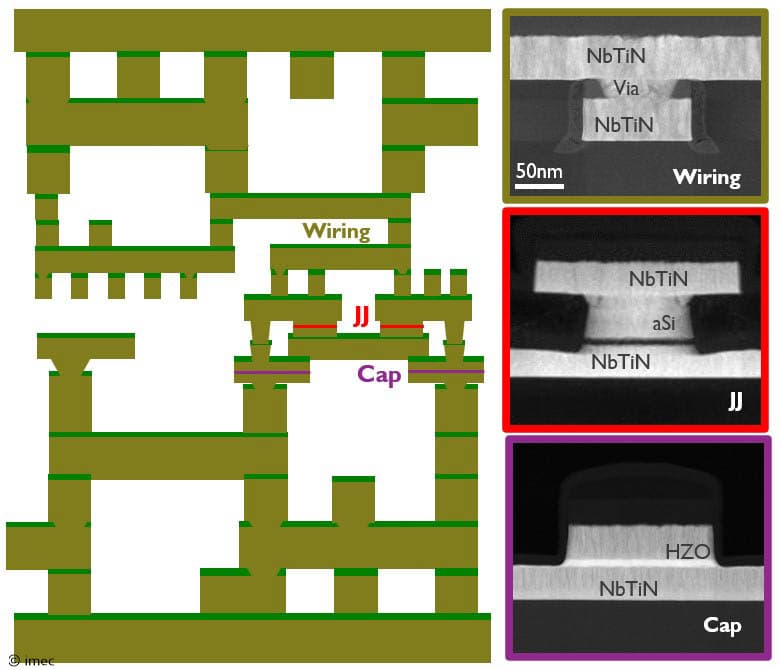
At 2024 IEDM, imec demonstrates functional NbTiN-based interconnects, Josephson junctions, and MIM capacitors fully compatible with CMOS processing and temperatures, with key metrics exceeding best-published results. For the superconducting interconnects, a semi-damascene integration process was used to build a two-metal-level scheme with wires and vias having critical dimensions down to 50 nm. Measurements at cryogenic temperatures reveal a critical temperature larger than 13K and a critical current density Jc>120 mA/µm2 – a world record at such a small scale. The Josephson junctions, with amorphous Si (aSi) sandwiched between two superconducting NbTiN layers, exhibit record-high Jc>2.5 mA/µm2. Imec researchers also demonstrated tunable HZO-based capacitors with NbTiN electrodes, having a high capacitance density of ~28 fF/µm2. With these characteristics, all three modules meet the process specifications in the envisioned system design.
“Key to the outstanding results is the adoption of novel integration schemes in combination with NbTiN, a superconducting material with much better scaling potential than Nb. The technology is scalable to high device densities, already exceeding superconducting state-of-the-art with 500x. Imec’s semi-damascene integration scheme is expandable to multiple metal levels. It lays the foundation for building a 16-metal-level interconnect fabric in which the junctions and capacitors must be embedded to benefit from the zero-wire resistance. The proposed technology can also withstand conventional BEOL processing temperatures (420°C) and is compatible with standard 300mm CMOS processing. We believe that our demonstration is a crucial step towards industrial processing in commercial foundries.”
About imec
Imec is a world-leading research and innovation center in nanoelectronics and digital technologies. Imec leverages its state-of-the-art R&D infrastructure and its team of more than 5,500 employees and top researchers, for R&D in advanced semiconductor and system scaling, silicon photonics, artificial intelligence, beyond 5G communications and sensing technologies, and in application domains such as health and life sciences, mobility, industry 4.0, agrofood, smart cities, sustainable energy, education, … Imec unites world-industry leaders across the semiconductor value chain, Flanders-based and international tech, pharma, medical and ICT companies, start-ups, and academia and knowledge centers. Imec is headquartered in Leuven (Belgium), and has research sites across Belgium, in the Netherlands, the UK and the USA, and representation in 3 continents. In 2023, imec's revenue (P&L) totaled 941 million euro.
Further information on imec can be found at www.imec-int.com.
Imec is a registered trademark for the activities of imec International and its affiliated entities.