Mitigating the thermal bottleneck in advanced interconnects
A modeling framework to accurately predict heat dissipation in the chip’s back-end-of-line

In short
As dimensional scaling continues, the heating of the interconnects in the chip’s back-end-of-line (BEOL) has become a growing concern, as it can compromise the chip’s reliability.
Imec presents a modeling framework that accurately predicts heat dissipation in advanced BEOL structures, considering the coupling with the logic cells in the front-end-of-line (FEOL) and boundary conditions from packaging technologies.
This article discusses the model and its added value. Valuable insights are presented, such as the dominant contribution of low-k dielectrics and via layers to the BEOL’s thermal resistance.
Scaling induced temperature rise in the BEOL: a growing concern
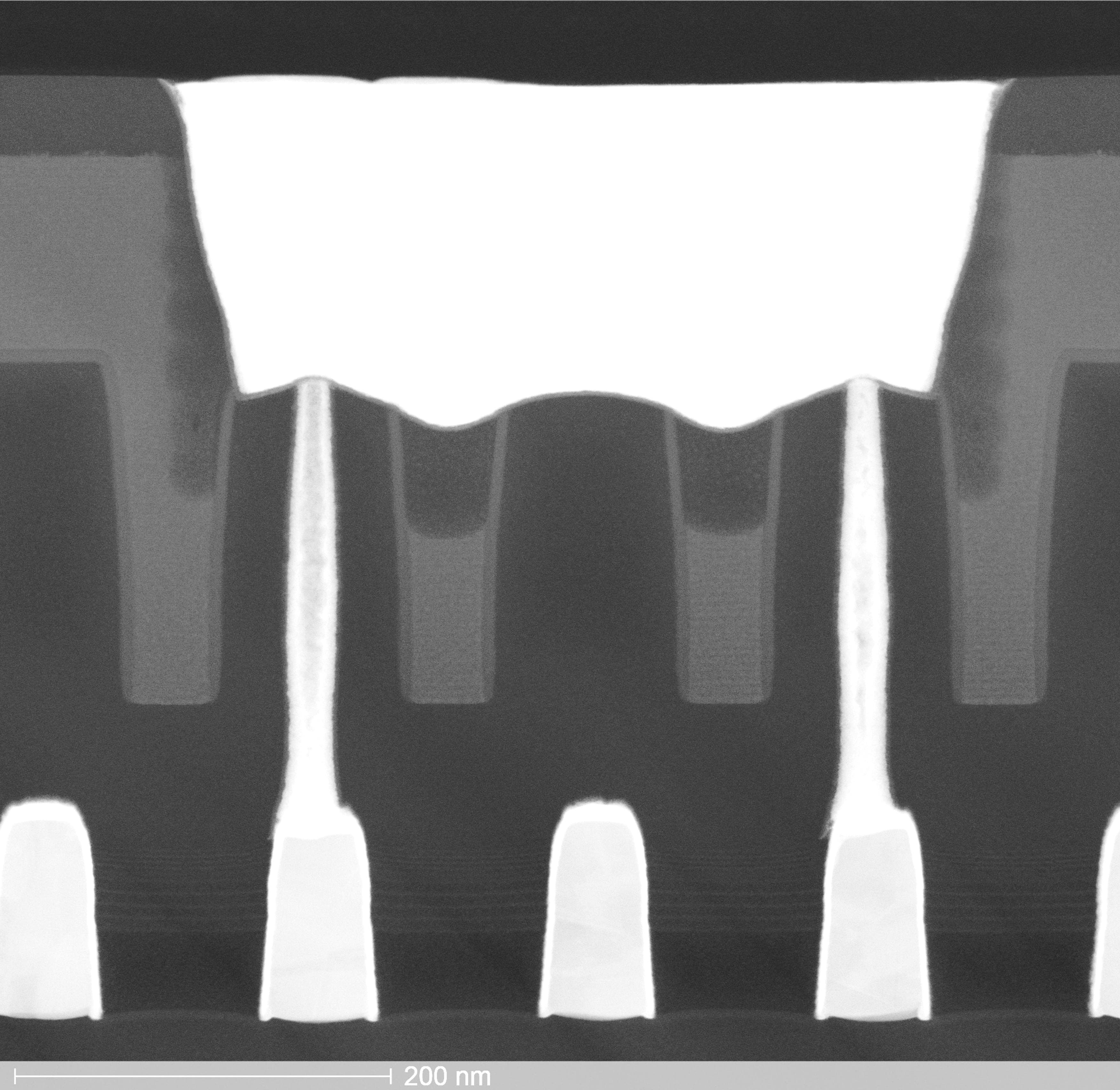
The back-end-of-line (BEOL) is a complex wiring scheme that distributes clock and other signals, provides power and ground, and transfers electrical signals from one transistor to another. It is organized in different metal layers containing local (Mx), intermediate (My), and (semi-)global interconnect wires (Mz). The total number of layers can be as many as 15, while the typical number of Mx layers ranges between 3 and 6. Each layer contains unidirectional metal lines, organized in regular tracks and surrounded by intermetal dielectrics. They are interconnected vertically using via structures that are filled with metal.
As dimensional scaling in the front-end-of-line (FEOL) continues, BEOL dimensions are also being reduced – leading to ever smaller metal pitches and reduced cross-sectional areas of the wires. Routing congestion and growing RC delay (resulting from an increased resistance-capacitance product (RC)) have become well-known bottlenecks for further interconnect scaling.
But the chip industry has for some time been concerned about another phenomenon: an increase in the BEOL’s thermal resistance and, with it, the heating up of the metal lines. This temperature increase can dramatically affect the reliability of the integrated circuits, as the reliability degradation of both the BEOL (related to electromigration and stress migration) and the FEOL (related to, e.g., negative bias temperature instability) is accelerated at high temperatures.
The main sources for heating are the active parts in the FEOL, the transistors, which dissipate energy during their operation. Nowadays, logic cells dissipate around 10W/mm2, and some of the generated heat is dissipated towards the neighboring BEOL [1,2]. On top of that, the currents that run through the interconnects for either power delivery or signal distribution also warm up the conductors, a phenomenon known as Joule heating. This worsens with each technology node due to a scaling-induced rise in the electrical resistivity of the interconnect metal lines and vias. The requirements for ever higher current densities and the poor thermal conductivity of the low-k dielectrics add to the problem.
The need for an accurate predictive framework
Traditionally, thermal analysis of FEOL and BEOL is performed separately using simplified models, and only the impact of the transistor on the first metal layer (M1) is considered. But this approach is becoming too narrow. The concern is fueled by emerging innovations that are expected to go against thermal improvement. Think about the introduction of air gaps as alternative dielectrics to improve RC delay or a further increase in the number of BEOL layers. Also, for 3D technologies, the BEOL might become the dominant contributor to the overall thermal resistance in advanced packages. The introduction of backside power delivery schemes (moving the entire power distribution network to the chip’s backside) and novel transistor architectures (such as gate-all-around nanosheets) in the logic roadmap may impact the temperature of the metal lines as well – in a good or bad sense.
A more comprehensive modeling framework is needed to capture the impact of these innovations on heat propagation and to enhance our fundamental understanding of how heat propagates in narrow BEOL structures. This framework should allow us to identify the biggest contributors to the warming up, predict how the BEOL’s thermal resistance evolves with newer technology nodes, and make recommendations for thermal-aware interconnect design.
A multi-step approach using calibrated models
Imec researchers take a modular approach to assess the thermal properties of the BEOL. They developed different types of models that capture the thermal properties of the materials at different dimensional scales and levels of detail. Each model can be used by itself, depending on the use case of interest. The output of each of the models can also be used as input for the next, enabling a complete analysis of a full BEOL stack. The modeling work is combined with experimental data obtained on test vehicles with industry-relevant materials and dimensions. The measured data are fed into the models, allowing for accurate calibration and prediction of future scenarios.
An overview of the different (sub-)models
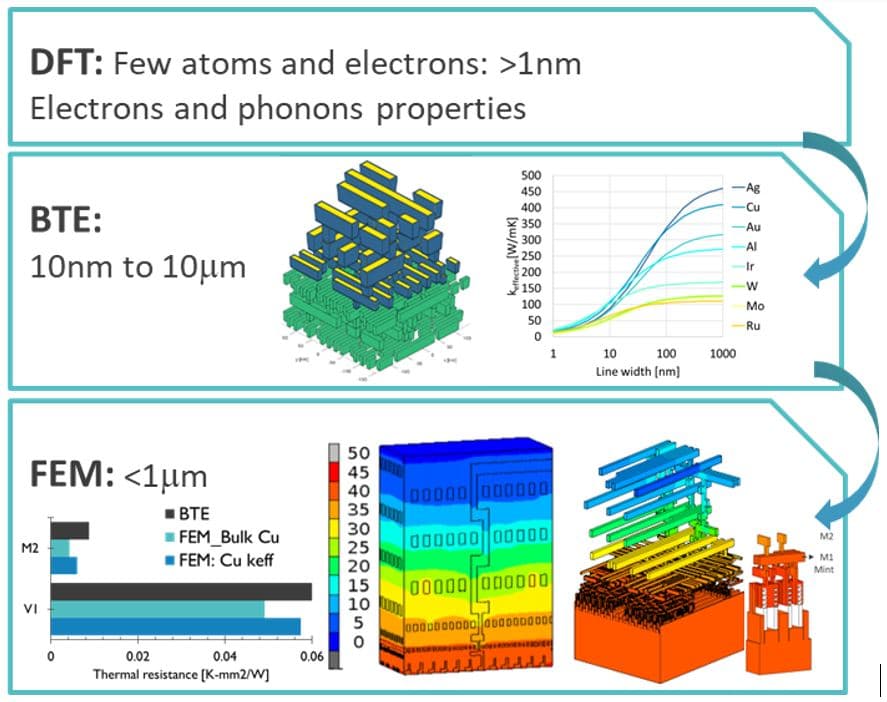
In the first step, the researchers investigate the materials at the atomic level using the density-functional theory (DFT). With this model, they derive fundamental properties of electrons and phonons, i.e., the heat carriers that move the energy inside the material.
In the next step, the heat conduction within the materials is modeled for varying material dimensions, from µm to nm scale. An in-house developed modeling tool is used that is based on the Boltzmann transport equation (BTE). The model additionally captures thermal effects at the nanoscale. The material properties of metals and dielectrics, as characterized on dedicated test structures, are used as an input for the model. For the dielectrics, for example, the so-called 3ω method was used to experimentally extract the thermal conductivity of relevant dielectric materials very precisely, revealing a value of 1.15W/mK for SiO2 and 0.3W/mK for OSG3.0 (an organosilicate glass with 3.0 dielectric constant).
In the third step, the researchers zoom out to a larger part of the BEOL layout. A full BEOL stack's thermal properties are modeled using a 3D finite element modeling (FEM) approach, calibrated with self-heating measurements. This final step gives a thermal conductivity/resistance mapping of the BEOL stack and its individual layers, allowing for a fast evaluation of the temperature rise in the interconnect structure.
To fully estimate how the heat propagates in the BEOL, the model must also accurately account for the heat exchange between the FEOL and BEOL. Imec researchers developed a methodology for estimating this heat exchange. This thermal coupling is added as an extra ‘layer’ to the FEM model.
Applying the models to different use cases: trends and useful insights
The thermal conductivity of elemental metals drops at <10nm line width
A typical outcome of the BTE modeling work is an evolution of the thermal conductivity of the materials with decreasing line widths. For all evaluated elemental metals, the thermal conductivity significantly drops when line widths scale into the 10nm region – relevant for the local level of interconnects at advanced technology nodes. This is illustrated in the graph in Figure 1 (middle).
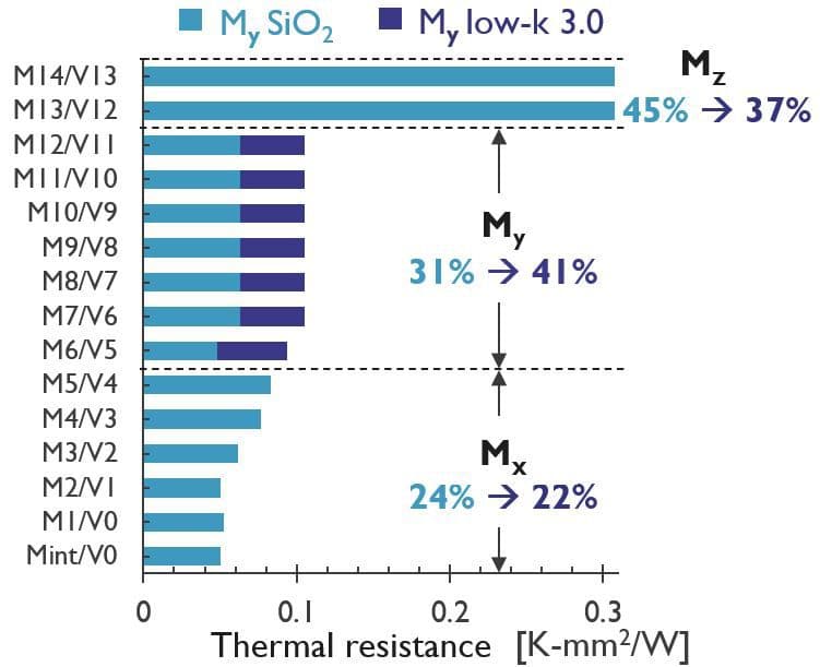
Low-k dielectrics, via layers and the My stack, dominate the thermal behavior of a 14-layer BEOL stack
The multi-step modeling framework was used to assess the thermal behavior of a complete, 14-layer BEOL stack in an advanced technology node. The work revealed interesting insights into the way the design and technology options for the BEOL impact the temperature rise.
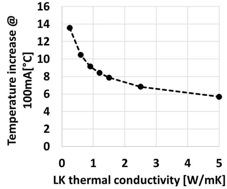
The contribution of the intermetal dielectric is significant. A fast temperature increase in the BEOL is observed when the thermal conductivity of the intermetal dielectric drops below 1W/mK. This is in the thermal conductivity range of most currently used dielectric materials such as OSG3.0. The impact worsens when air gaps are introduced (e.g., in the A14 technology node) due to the very poor thermal conductivity of the air gap: simulations show an increase of 30 percent for the metal line self-heating. The (choice of the) metal, on the contrary, has a minimal impact on thermal dissipation.
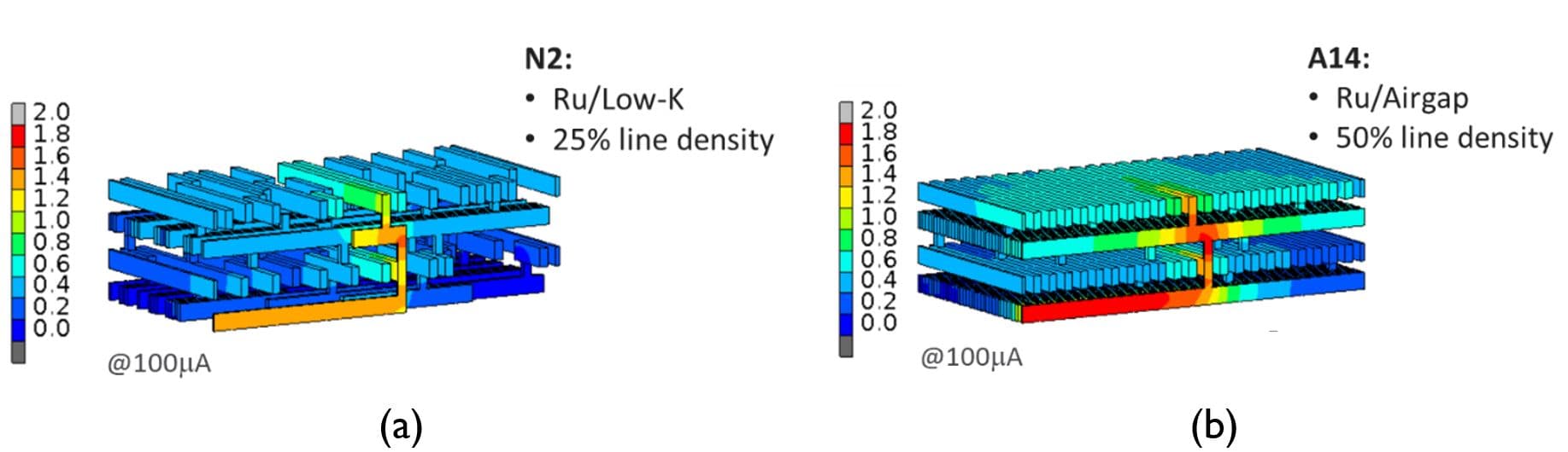
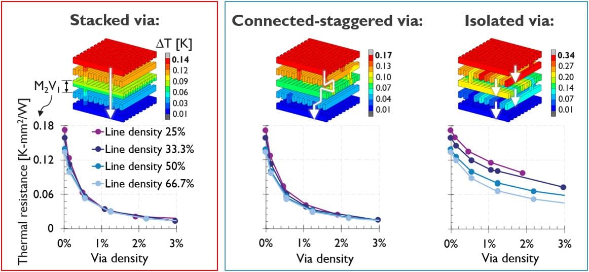
The impact of the via density and configuration cannot be ignored. A larger via density is found to favor thermal dissipation between interconnect layers. The same applies to a stacked via configuration, where vias between different layers are nicely aligned. Such a configuration is typically applied in the global interconnect layers (Mz) used for power delivery. A more randomized configuration, commonly used for signal routing in Mx and My layers, contributes to increased heating of the interconnect layers.
Finally, when low-k materials are used as intermetal dielectrics in the My layers, the My stack dominates the thermal resistance of the full BEOL stack. Consequently, the My part of the BEOL stack provides the most significant opportunity for thermal optimization. The analysis also confirms the impact of the via layers: for the 14-layer stack, they contribute to 86 percent of the total thermal resistance of the BEOL stack, while the line layers only give 14 percent. Note that the thermal resistance of a layer is defined as its thickness divided by the thermal conductivity.
Heat exchange between FEOL and BEOL strongly depends on the package and cooling solution
The metal line temperature is a combination of the line self-heating in the BEOL stack and the heating in the FEOL. The heat exchanged between FEOL and BEOL highly depends on how the chip is packaged and on the solution provided for cooling the package – hence, on the application. Our model was evaluated on three flip-chip packages having different cooling scenarios.
In the first scenario, an over-molded flip-chip package is cooled via natural convection from the top of the package, which is closest to the FEOL. In a second scenario, a metal lid frame is added to improve the heat conduction to the upper part. In a third case, forced cooling is applied on the top. While the first and second scenarios resemble a mobile application, forced cooling is typically used in high-performance computer applications.
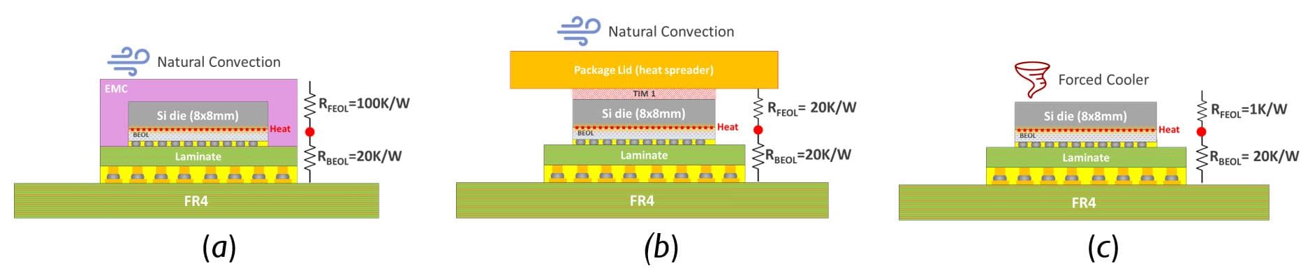
For the first scenario, most of the heat generated in the FEOL is removed via the BEOL towards the laminate on which the flip-chip package is attached. In other words, this cooling solution results in a large thermal resistance for the FEOL and the BEOL self-heating. The second and third scenarios improve the thermal path towards the top resulting in a 40 percent and 90 percent temperature reduction respectively, for the same FEOL power, while the BEOL self-heating only reduces slightly.
A valuable tool for STCO
As explained above, each presented model can be deployed for specific use cases, depending on the dimensional scale of interest. For example, the FEM model can be applied to simplified BEOL stacks to investigate thermal aspects of more advanced metallization schemes at the local level, such as semi-damascene. Also, alternative routing and power delivery schemes – such as backside power delivery – can be assessed by feeding in different package configurations in the package model.
Ultimately, mitigating the thermal bottleneck in the chip’s BEOL will bring system performance benefits for targeted applications. As such, the models proposed in this work will help identify the right technology ingredients that can unlock major system scaling bottlenecks. They will provide valuable input for imec’s 3D and design-technology co-optimization (DTCO) work and, eventually, for the system-technology co-optimization (STCO) that starts from system application needs.
This article was originally published in Chip Scale Review – September-October 2023 (pgs 43-48).
Want to know more?
The results presented in this article are described in more detail in the following papers. Interested in receiving a copy? Fill in our contact form.
[1] ‘Towards accurate temperature prediction in BEOL for reliability assessment,’ M. Lofrano et al., IRPS 2023 (Invited);
[2] ‘Calibrated fast thermal calculation and experimental characterization of advanced BEOL stacks,’ X. Chang et al., IEEE IITC/MAM 2023.
Authors

Melina Lofrano
Melina Lofrano is a research engineer in the thermal modeling and characterization team at imec. She holds an M.Sc. in mechanical engineering from the University of São Paulo, Brazil. In 2008 she joined imec, Belgium, where she has been working with thermal and mechanical analysis for micro and nanoelectronic reliability. Her activities cover multiple topics, including thermal and thermomechanical analysis of back-end-of-line interconnect, 3D IC assembly, chip package interaction, MEMS resonators, GaN devices, and non-linear material characterization. Currently, she works on thermal analysis for 3D system integration and is responsible for the nano IC thermal modeling and characterization activities

Xinyue Chang
Xinyue Chang is a Ph.D. researcher at imec and KU Leuven, focusing on thermal modeling and experimental characterization of advanced back-end-of-line (BEOL) structures. She received her M.Sc. degree in electronic and communication engineering from Shanghai Jiao Tong University, Shanghai, China, in 2019. Soon after, she joined imec’s thermal modeling and characterization team and is currently pursuing a Ph.D. degree with KU Leuven.

Herman Oprins
Herman Oprins is a senior research engineer at imec in Leuven, Belgium. He received the M.Sc and Ph.D. degrees in Mechanical Engineering from the K.U. Leuven, Belgium. He joined imec in 2003, pursuing the PhD degree, working on the development and modeling of an electrowetting assisted cooling technique. In that period he also worked on modeling and experimental projects in the field of thermal management of electronic packages. Since 2009 he is a senior research engineer in imec, where he is involved in the thermal experimental characterization, thermal modeling and thermal management of 3D system integration, electronic chip packages, BEOL, Si photonics and GaN power transistors.

Zsolt Tokei
Zsolt Tokei is Distinguished Member of Technical Staff Interconnects at imec. He joined imec in 1999 and since then held various technical positions in the organization. First as a process engineer and researcher in the field of copper low-k interconnects, then he headed the metal section. Later he became principal scientist, Program Director Nano-Interconnects and, in 2016, was appointed Distinguished Member of Technical Staff Interconnect. He earned a M.S. (1994) in physics from the University Kossuth in Debrecen, Hungary. In the framework of a co-directed thesis between the Hungarian University Kossuth and the French University Aix Marseille-III, he obtained his PhD (1997) in physics and materials science. From 1998 he worked at the Max-Planck Institute of Düsseldorf, Germany, as a post-doctorate researcher. From the date of joining imec he continued working on a range of interconnect issues including scaling, metallization, electrical characterization, module integration, reliability and system aspects.