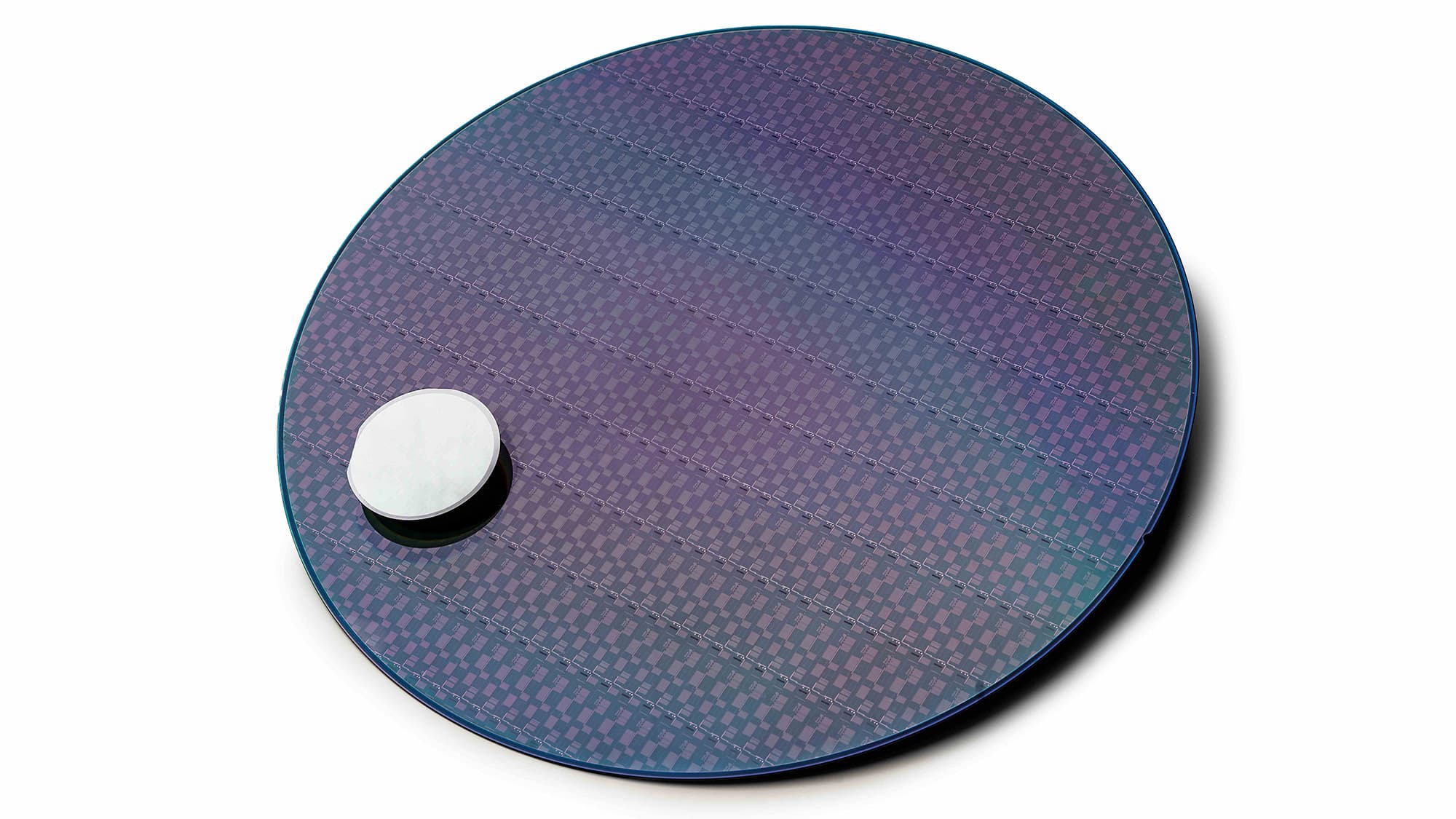
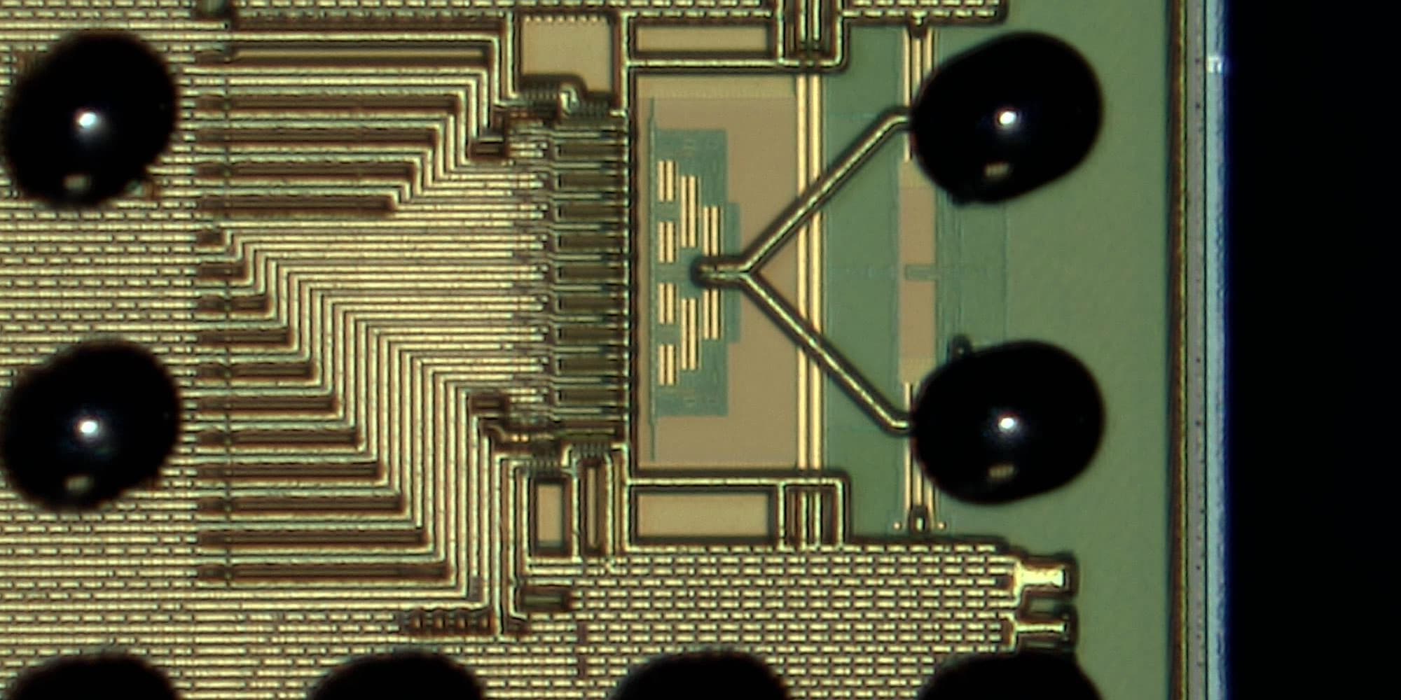
Imec introduces simulation framework to better predict thermal transport in RF devices for 5G and 6G.
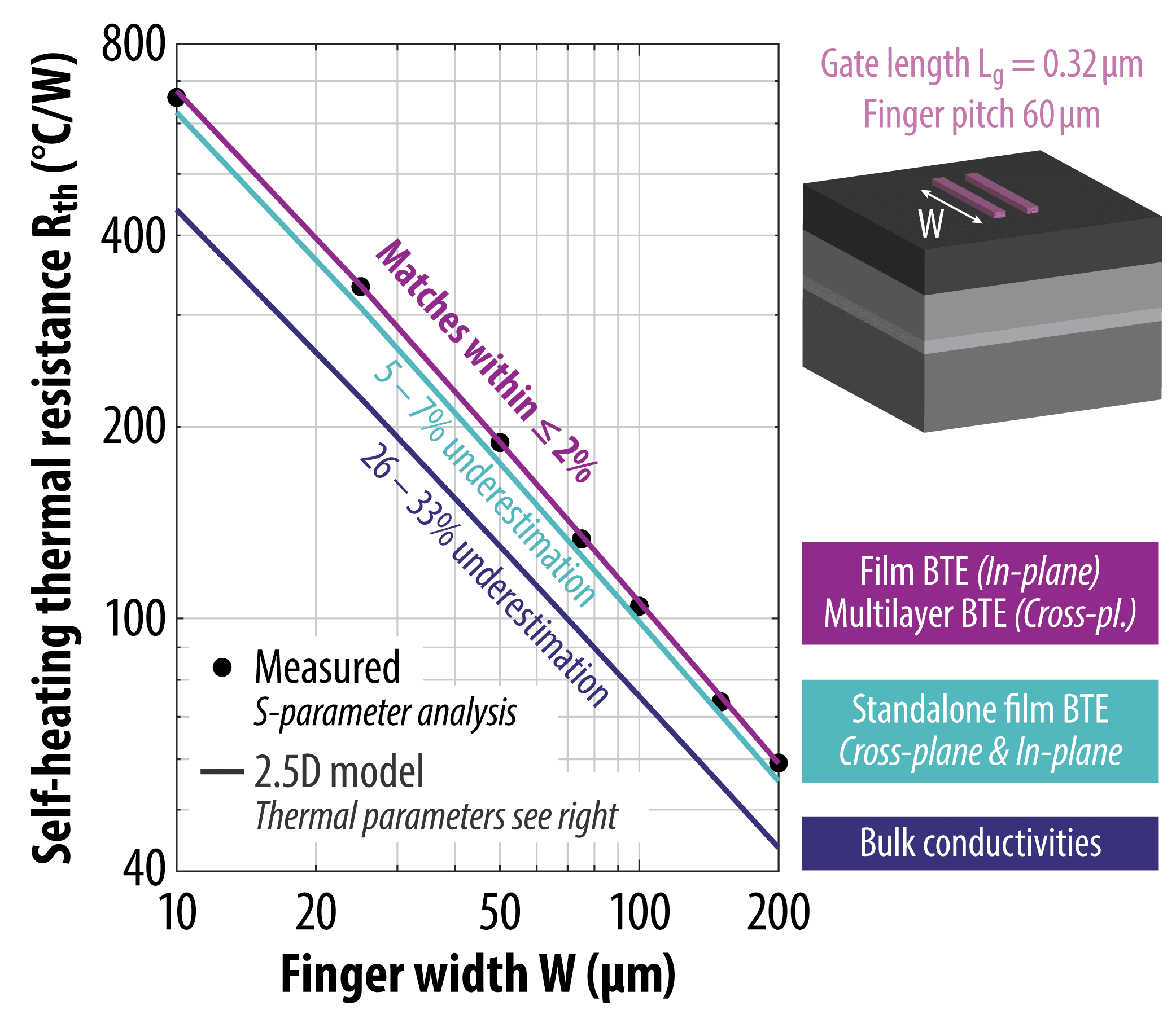
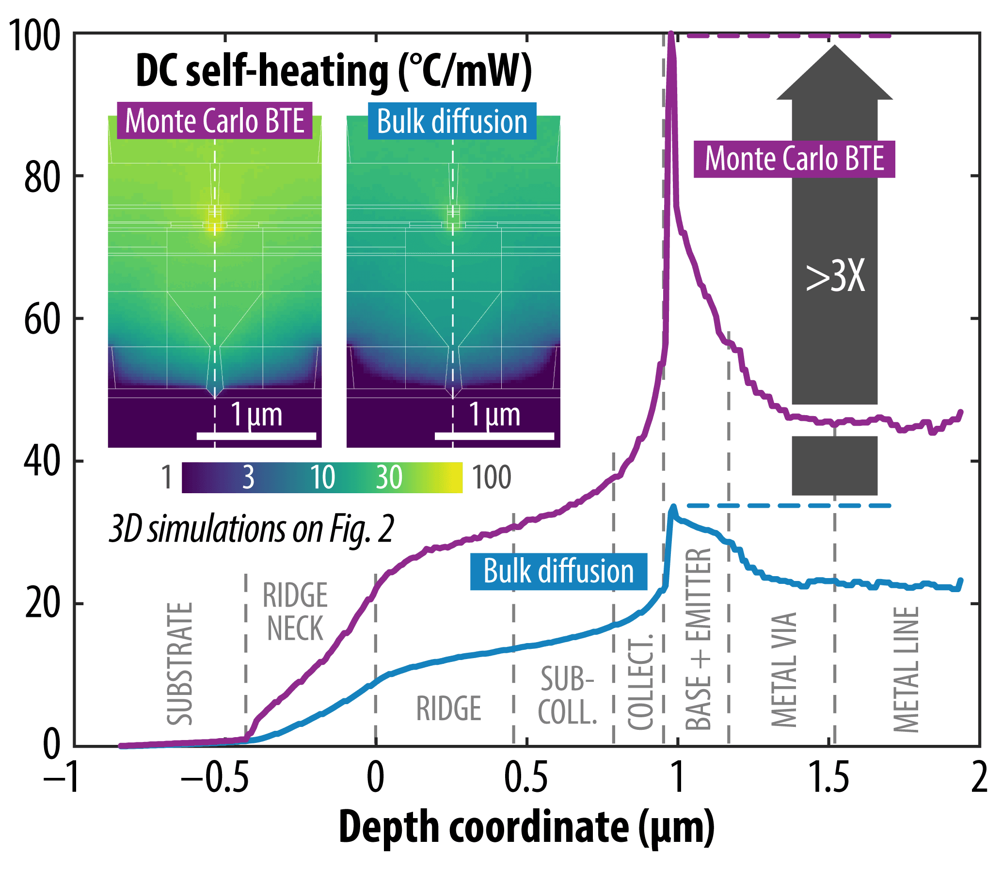
LEUVEN (Belgium), December 6, 2022— This week, at the 2022 International Electron Devices Meeting (IEEE IEDM 2022), imec, a world-leading research and innovation hub in nanoelectronics and digital technologies, presents a Monte Carlo Boltzmann modeling framework that uses microscopic heat carrier distributions to predict 3D thermal transport in advanced RF devices intended for 5G and 6G wireless communication for the first time. Case studies with GaN high-electron-mobility transistors (HEMTs) and InP heterojunction bipolar transistors (HBTs) revealed peak temperature rises that are up to three times larger than conventional predictions with bulk material properties. Imec’s new tool will be very useful in guiding optimizations of next-gen RF devices toward thermally improved designs.
GaN- and InP-based devices have emerged as interesting candidates for 5G mm-wave and 6G sub-THz mobile front-end applications, respectively, due to their high output power and efficiency. To optimize these devices for RF applications and make them cost-effective, much attention is paid to upscaling the III/V technologies to a Si platform and making them CMOS compatible. However, with shrinking feature sizes and rising power levels, self-heating has become a major reliability concern, potentially limiting further RF device scaling.
Nadine Collaert, program director of advanced RF at imec: “Tuning the design of GaN- and InP-based devices for optimal electrical performance often worsens thermal performance at high operating frequencies. For GaN-on-Si devices, for example, we recently achieved tremendous progress in electrical performance, bringing the power-added efficiencies and output power for the first time on par with that of GaN-on-silicon carbide (SiC). But further enlarging device operating frequency will require downsizing the existing architectures. In these confined multilayer structures, however, thermal transport is no longer diffusive, challenging accurate self-heating predictions. Our novel simulation framework, yielding good matches with our GaN-on-Si thermal measurements, revealed peak temperature rises up to three times larger than previously predicted. It will provide guidance in optimizing these RF device layouts early in the development phase to ensure the right trade-off between electrical and thermal performance.”
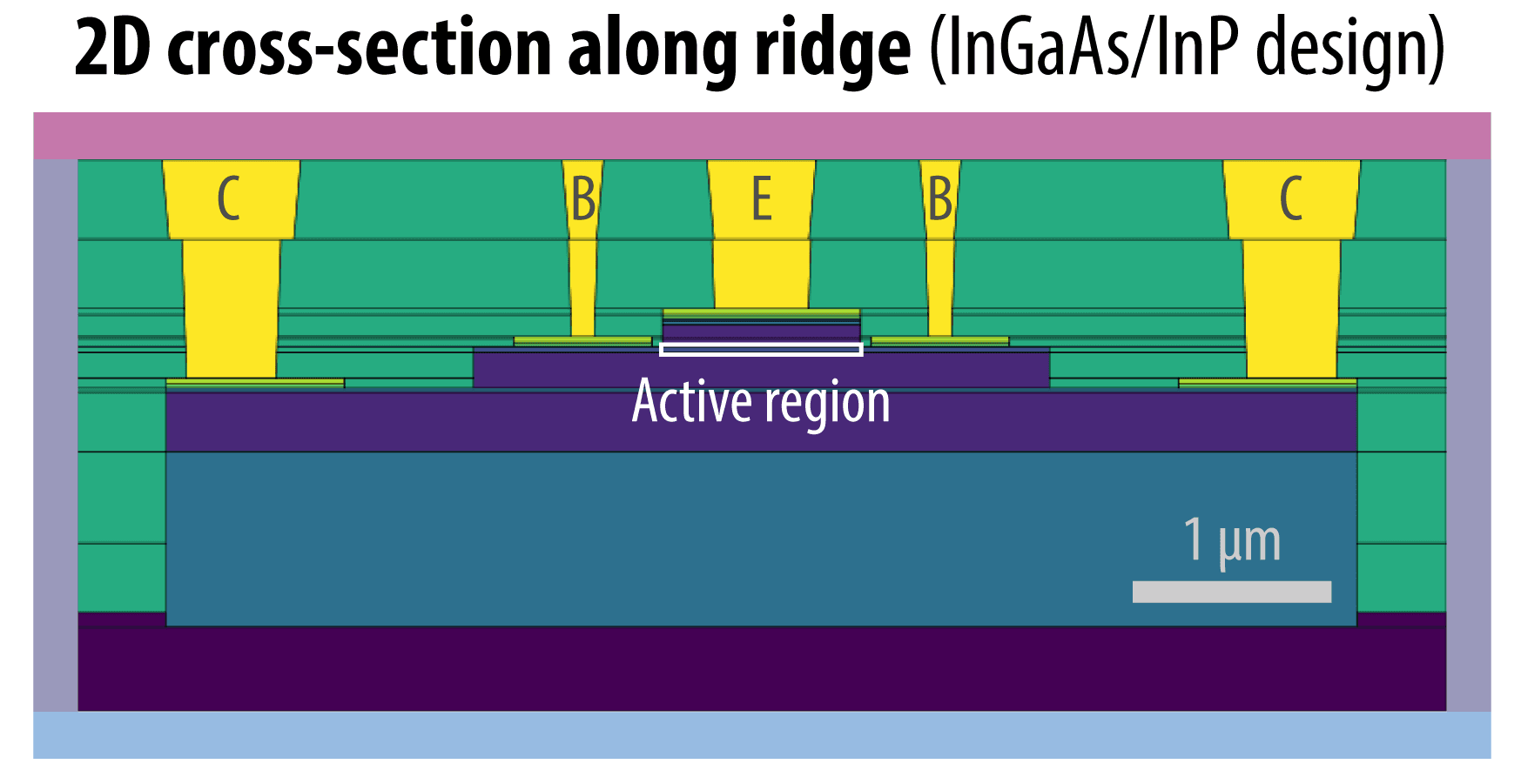
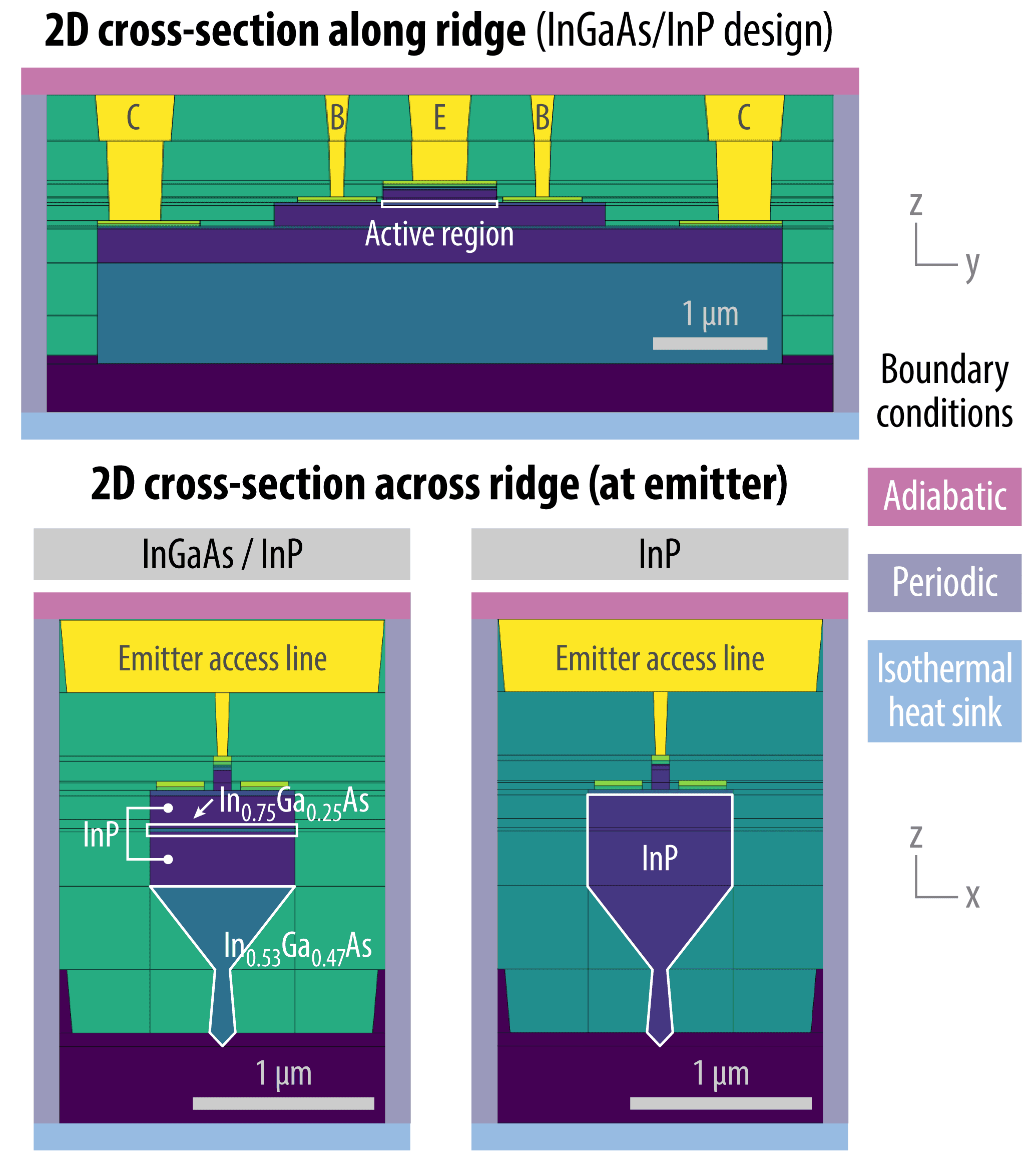
Such guidance also proves very valuable for the novel InP HBTs, where imec’s modeling framework highlights the substantial impact non-diffusive transport has on self-heating in complex scaled architectures. For these devices, nanoridge engineering (NRE) is an interesting heterogeneous integration approach from an electrical performance point of view. “While the tapered ridge bottoms enable low defect density within the III-V materials, they, however, induce a thermal bottleneck for heat removal towards the substrate,” explains Bjorn Vermeersch, principal member of technical staff in the thermal modeling and characterization team at imec. “Our 3D Monte Carlo simulations of NRE InP HBTs indicate that the ridge topology raises the thermal resistance by over 20 percent compared to a hypothetical monolithic mesa of the same height. Our analyses furthermore highlight the direct impact of the ridge material (e.g., InP vs. InGaAs) on self-heating, providing an additional knob to improve the designs thermally.”
These results are presented in two invited papers at the 2022 IEDM, by Bjorn Vermeersch, on thermal modeling, and by Nadine Collaert, on GaN and InP technologies for next-generation high-capacity wireless communication, respectively [papers 11.5 and 15.3].
About imec
Imec is a world-leading research and innovation center in nanoelectronics and digital technologies. Imec leverages its state-of-the-art R&D infrastructure and its team of more than 5,000 employees and top researchers, for R&D in advanced semiconductor and system scaling, silicon photonics, artificial intelligence, beyond 5G communications and sensing technologies, and in application domains such as health and life sciences, mobility, industry 4.0, agrofood, smart cities, sustainable energy, education, … Imec unites world-industry leaders across the semiconductor value chain, Flanders-based and international tech, pharma, medical and ICT companies, start-ups, and academia and knowledge centers. Imec is headquartered in Leuven (Belgium), and has research sites across Belgium, in the Netherlands and the USA, and offices in China, India, Taiwan and Japan. In 2021, imec's revenue (P&L) totaled 732 million euro.
Further information on imec can be found at www.imec-int.com.
Imec is a registered trademark for the activities of imec International (IMEC International, a legal entity set up under Belgian law as a “stichting van openbaar nut”), imec Belgium (IMEC vzw supported by the Flemish Government), imec the Netherlands (Stichting IMEC Nederland), imec Taiwan (IMEC Taiwan Co.), imec China (IMEC Microelectronics (Shanghai) Co. Ltd.), imec India (IMEC India Private Limited), imec San Francisco (IMEC Inc.) and imec Florida (IMEC USA Nanoelectronics Design Center Inc.).
Discover more