Heterogeneous integration technologies to enable the next generation of wireless 6G
InP shows promise to power 6G technology. Heterogeneous integration is key to its advancement, co-integrating all components into a cohesive system.

In short
The future 6G asks for materials and devices that can operate at >100GHz.
Indium Phosphide (InP) can deliver the required speed, efficiency, and output power.
For future use of InP technology, imec explores nano-ridge engineering to grow InP on silicon.
To co-integrate all components into a communication circuit, imec is looking into PCBs, 2.5D, and 3D methods
Technology for the future generations of mobile communication
Every ten years heralds a new generation of mobile communication. Over the generations, the number of subscribers has grown tremendously, with each consuming an ever-increasing amount of wireless data. “In the beginning, we were happy to be able to send a text message; today, we’ve reached the 5th generation (5G) with more than a billion human-to-machine and machine-to-machine connections with peak data rates of 10Gbits/sec. 5G is also an inflection point. Because in addition to needing more data and more connections at ever higher speed, we must now consider how to enable new use cases such as autonomous driving and holographic presence. That trend will continue moving into 6G, which is envisioned for 2030. There, we expect peak data rates higher than 100Gbits/sec, extreme coverage, pervasive connectivity, and more,” says Michael Peeters, VP of R&D for connectivity at imec.
Indium Phosphide delivers power and efficiency at high frequencies
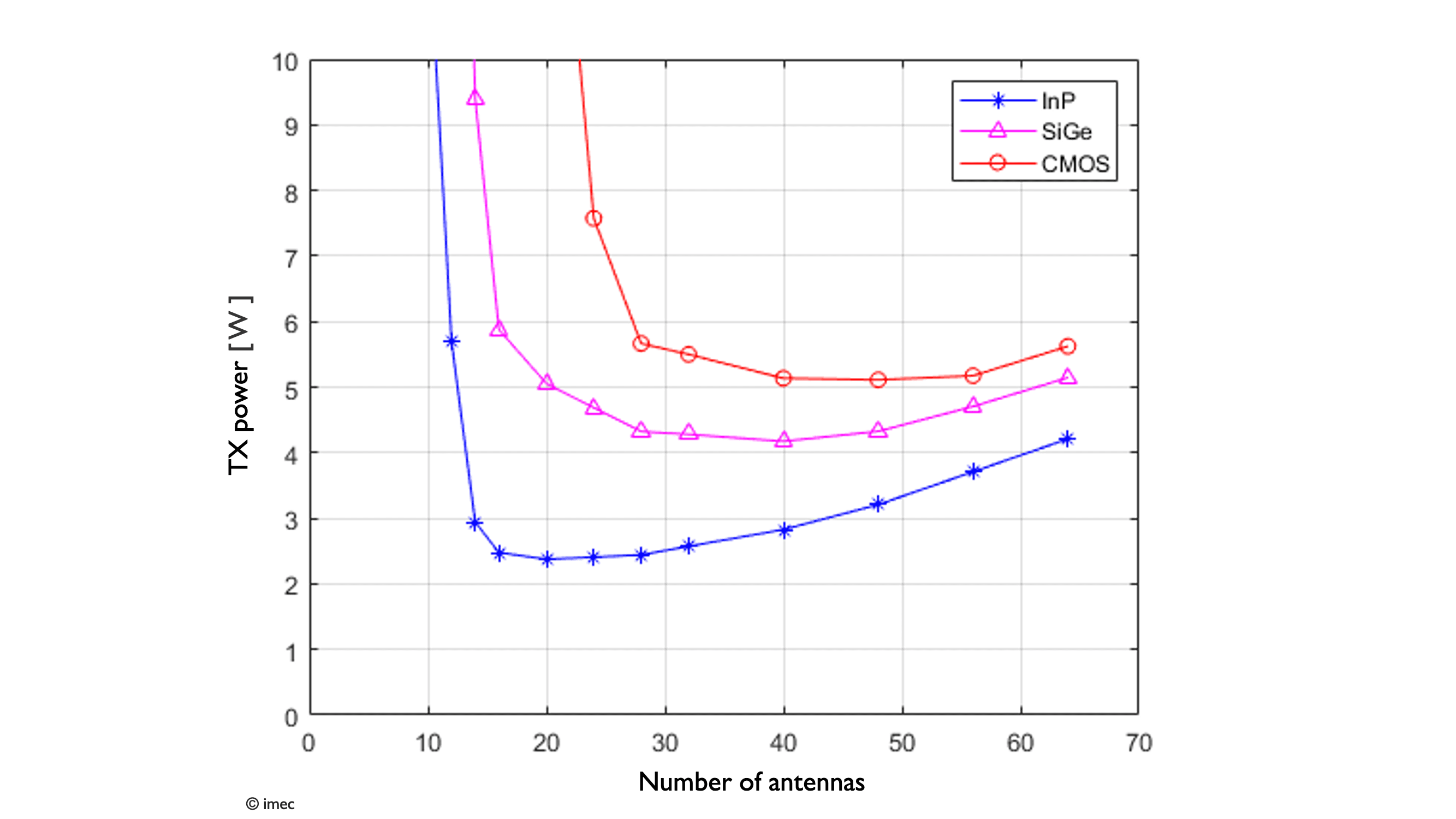
In order to enable these very high data rates, the telecom industry has been pushing the frequencies up. The vision for 6G is that frequencies above 100GHz –starting with the D-band around 140GHz– will be addressed. Michael Peeters: “We believe the biggest challenge above 100GHz is to generate sufficient power with sufficiently high efficiency. For both CMOS and SiGe amplifiers, the saturated output power in the D-band does not exceed 15dBm, and the efficiency is typically below ten percent, which is very low, given that popular modulation schemes like 64-QAM need to operate more than 6dB below that saturated output power. The efficiency also drops more than linearly with the output power. Indium Phosphide (InP) is the champion at these frequencies, with an output power of over 20dBm and efficiencies ranging from 20 to even 30 percent. InP can deliver performance at the high frequencies required. Especially when you are footprint-restricted and can only accommodate a limited number of antennas, InP takes the lead enabling a two times lower power consumption at an even two times smaller footprint.”
Envisioning InP technology
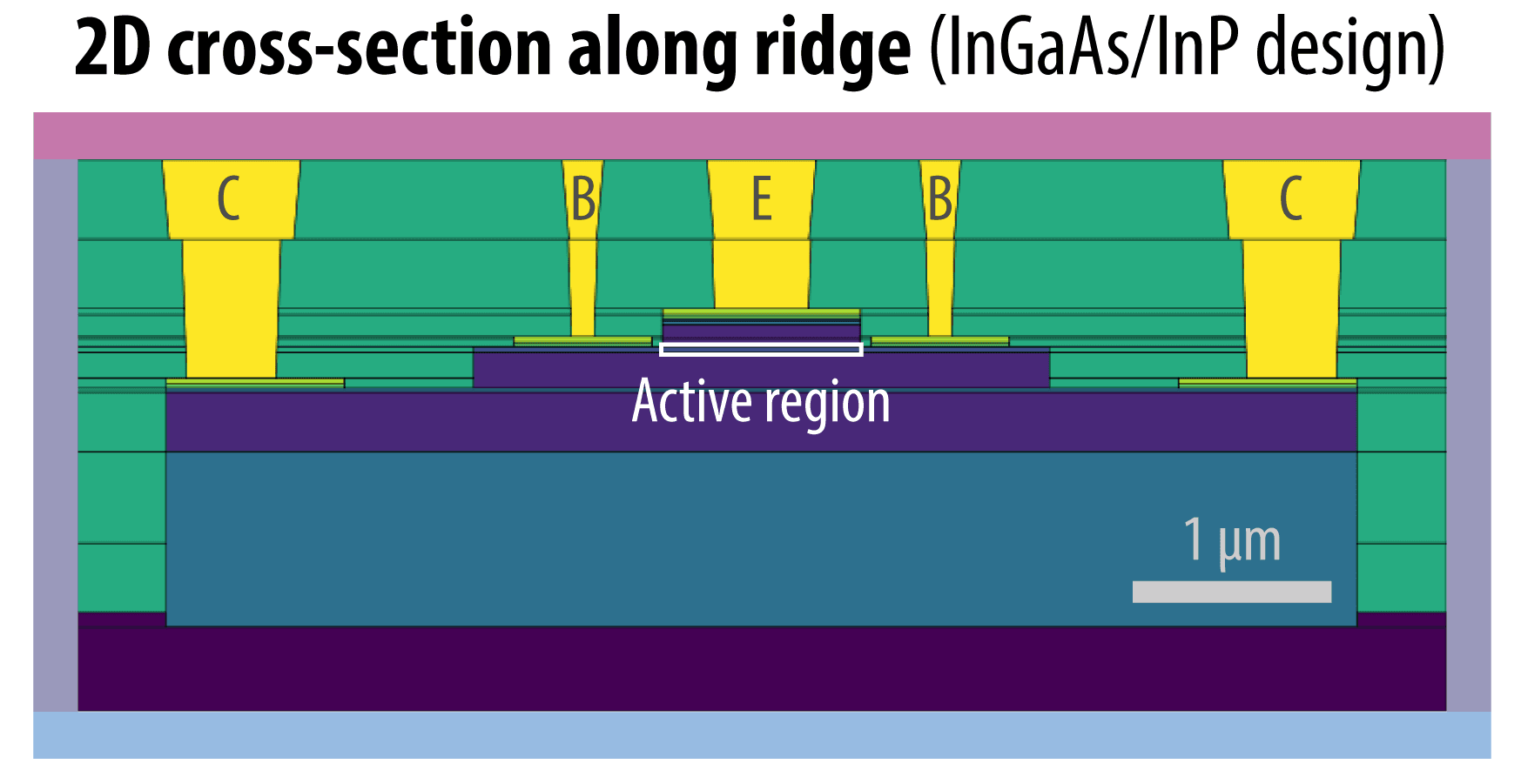
If we want to implement InP as a 6G solution on the longer term, a few technological hurdles need to be taken. Creating InP transistors (HBT, heterojunction bipolar transistor) that can handle high frequencies requires, first, a mature and cost-efficient InP technology and, second, an approach to co-integrate InP-based components with silicon-based components into a complete system. For both challenges, the heterogeneous integration of a III-V material such as InP with CMOS is key. After all, CMOS will still be needed for calibration, control, beamforming, and convertors.
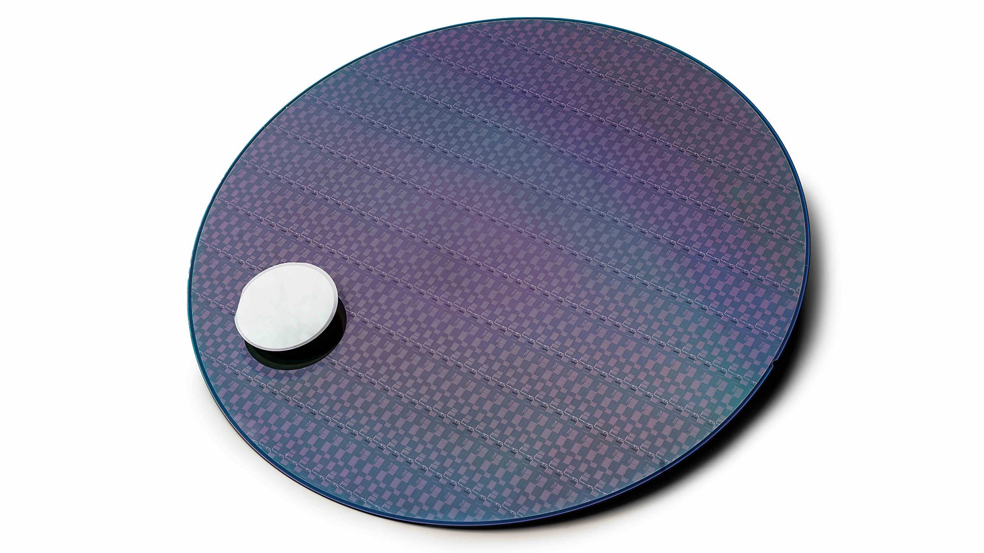
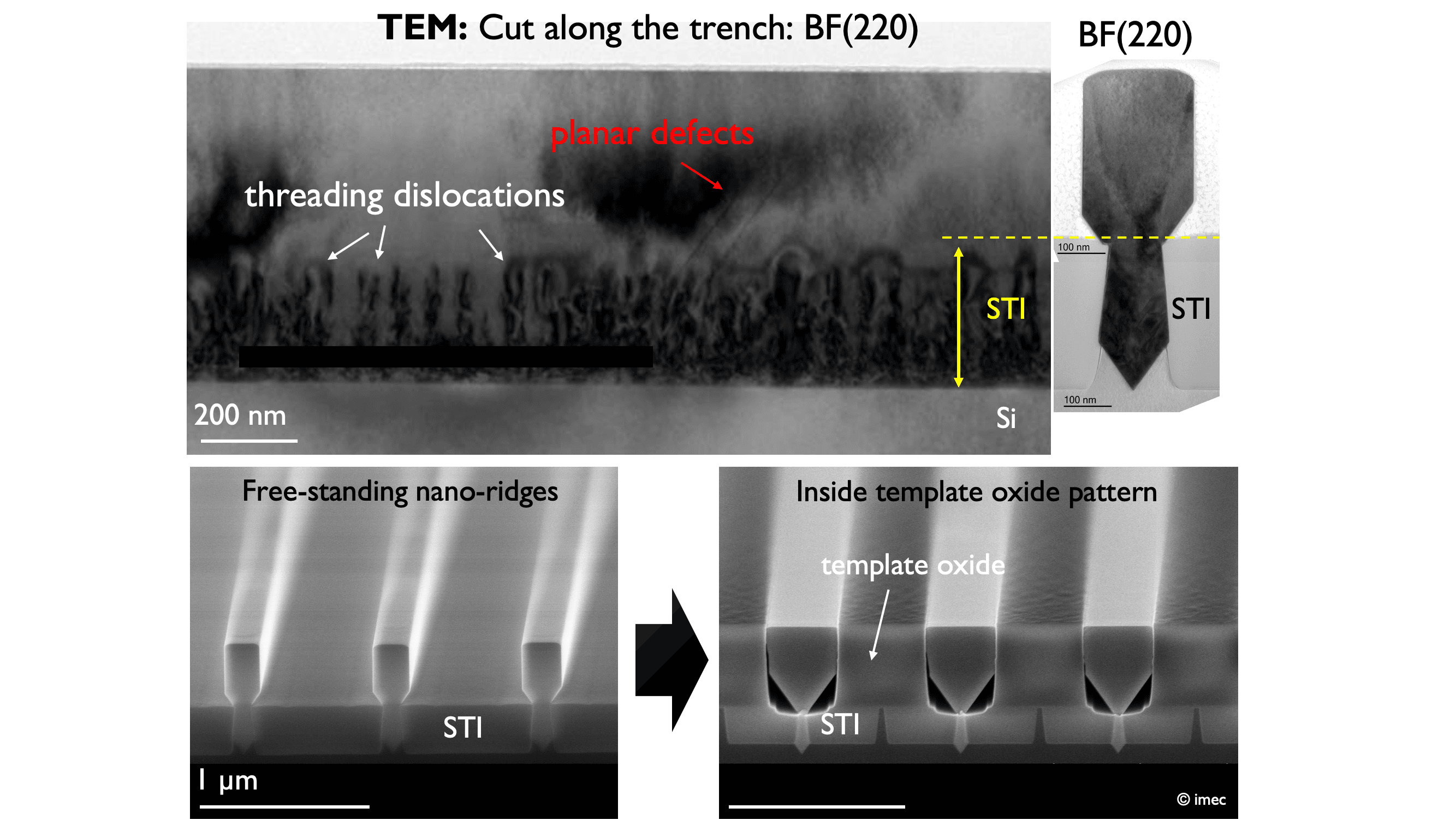
Today, InP technology comes in small substrate wafers (<6inch), is based on lab-like processes such as e-beam, and uses gold-based contacts which are not CMOS-compatible. Being able to handle the brittleness of InP is one of the most prominent challenges. Imec is exploring technologies to transfer III-V materials onto a cheaper and more robust substrate, like silicon. Due to the large lattice mismatch between both materials, growing InP on silicon usually goes along with the introduction of defects, mainly threading dislocations and planar defects. These defects induce leakage currents, which can dramatically deteriorate device performance or cause problems with reliability because defects can capture and release carriers at high RF frequencies.
Nano-ridge engineering traps defects in InP grown on silicon
To address the defects that occur while directly growing InP on silicon, imec is looking at so-called nano-ridge engineering, a process that relies on selectively growing the III-V material in pre-patterned structures or trenches in the silicon. These high-aspect-ratio trenches are very effective in trapping the defects in the narrow bottom part and in allowing the growth of high-quality, low-defectivity material out of the trench. At the same time, overgrowing the nano-ridge widens it towards the top, forming a solid base for a device stack. If you reduce the pitch between the nano-ridges, you can even merge them to create a plate of III-V material locally.
“Recently, imec demonstrated InGaAs 53% box-shaped nano-ridges that could efficiently trap threading dislocations in the trench. The nano-ridges were successfully grown both standalone and in a guided template. We are investigating the same approach, combining InGaAs nano-ridge engineering with the insights from earlier demonstrations of InGaP/GaAs nano-ridge HBTs to develop a needed heterostructure stack for 140GHz applications. To address the challenges related to speed, efficiency, and output power needed for the next generations of wireless high data rate communication systems, we envision InP HBTs on a 300mm Si wafer platform,” says Nadine Collaert, program director of the advanced RF program at imec.
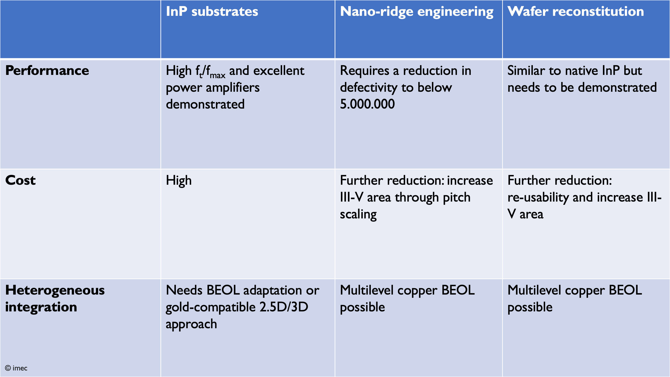
Aside from the direct growth approaches such as nano-ridge engineering, InP can also be placed on silicon through integration schemes that still rely on small-sized InP substrates as the starting material. There, high-quality InP substrates are diced and sorted into non-patterned tiles in a process called wafer constitution. The tiles are subsequently attached to a silicon wafer, planarized, and processed in the fab. Both the direct growth and wafer reconstitution options have pros and cons regarding performance, cost, and heterogeneous integration potential.
Co-integration approaches on a system-level
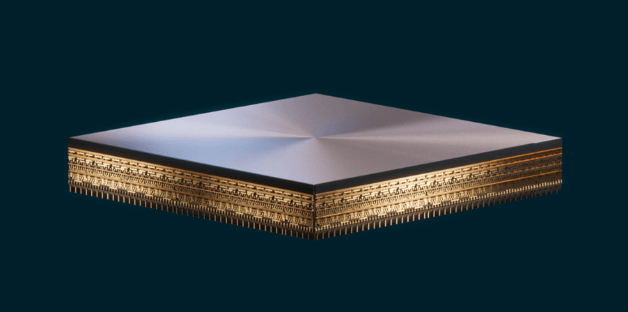
Obtaining a mature and cost-efficient InP technology through direct growth or wafer reconstitution is only part of the challenge. The resulting components eventually need to be integrated into a complete system, made up of building blocks in a combination of III-V and CMOS-based technologies, such as InP HBTs (for power amplifiers) or CMOS (for the beamforming transceiver). This need brings about a whole set of integration challenges. Imec is looking into monolithic (2D) integration of III-V devices with silicon devices in the same plane and into 2.5D and 3D integration technologies to achieve heterogeneous integration.
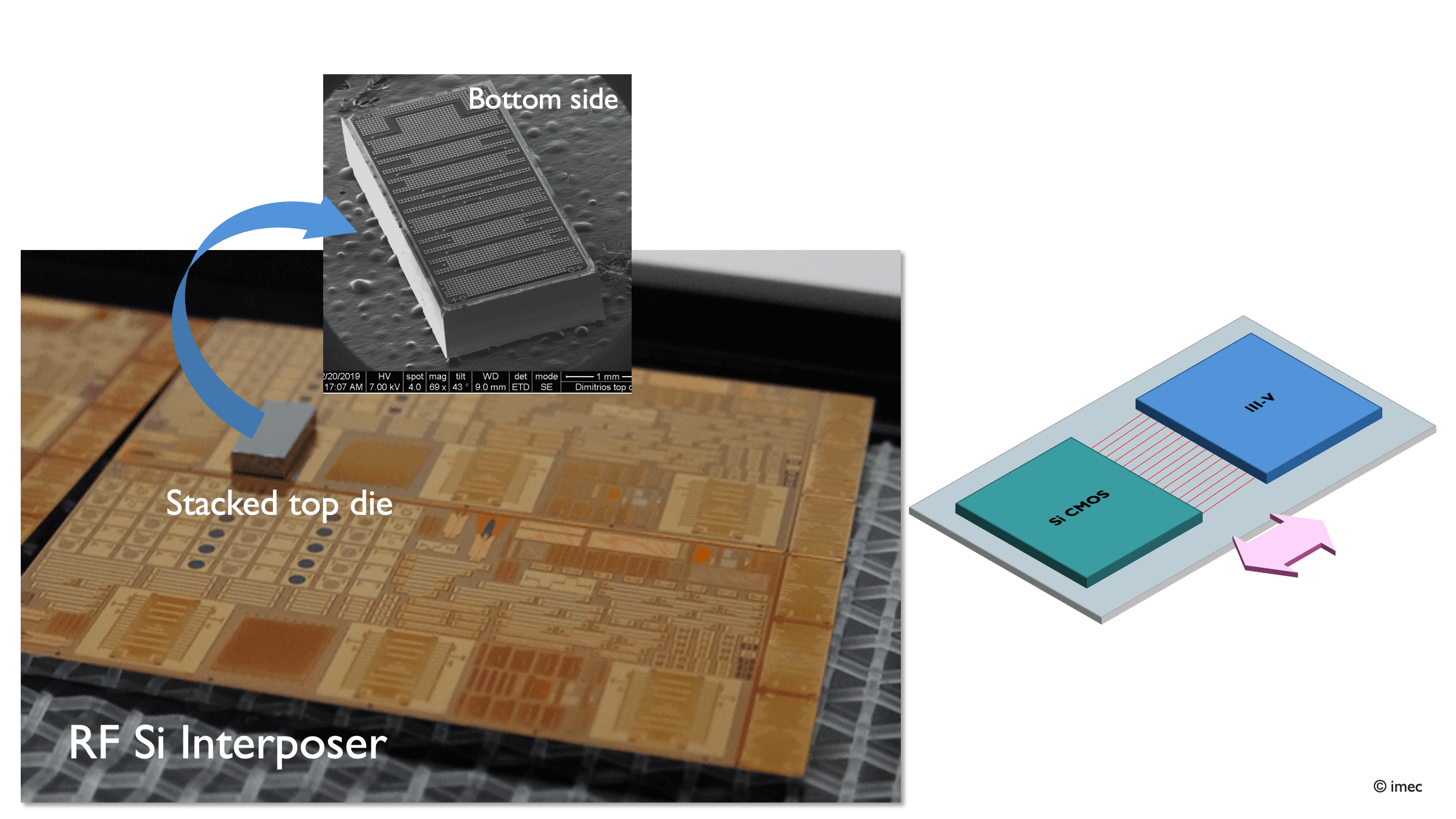
The PCB (printed circuit board) is still state-of-the-art technology, and optimizations to make it amendable to higher frequencies are ongoing. These efforts include reducing the pitch and optimizing materials and layout. 2.5D integration utilizes silicon interposers (a chip or layer with lithography-defined connections and even through-silicon via’s) to communicate between a III-V and a silicon chip. “The technology is already optimized for high-speed digital applications but requires more work to make it a solution for RF applications. Specifically, we are evaluating different options of dielectrics and thickness of the metal layers to enable low-loss interconnects. We need either high resistive silicon substrates or thick dielectric layers to distance the metal layers from the lossy substrate, but also very thick RDL (redistribution layer), an extra metal layer to reduce the metal loss. We will also look at integrating high-quality passives for certain cases,” explains Nadine Collaert.
2.5D and 3D technologies as key enablers for heterogeneous integration
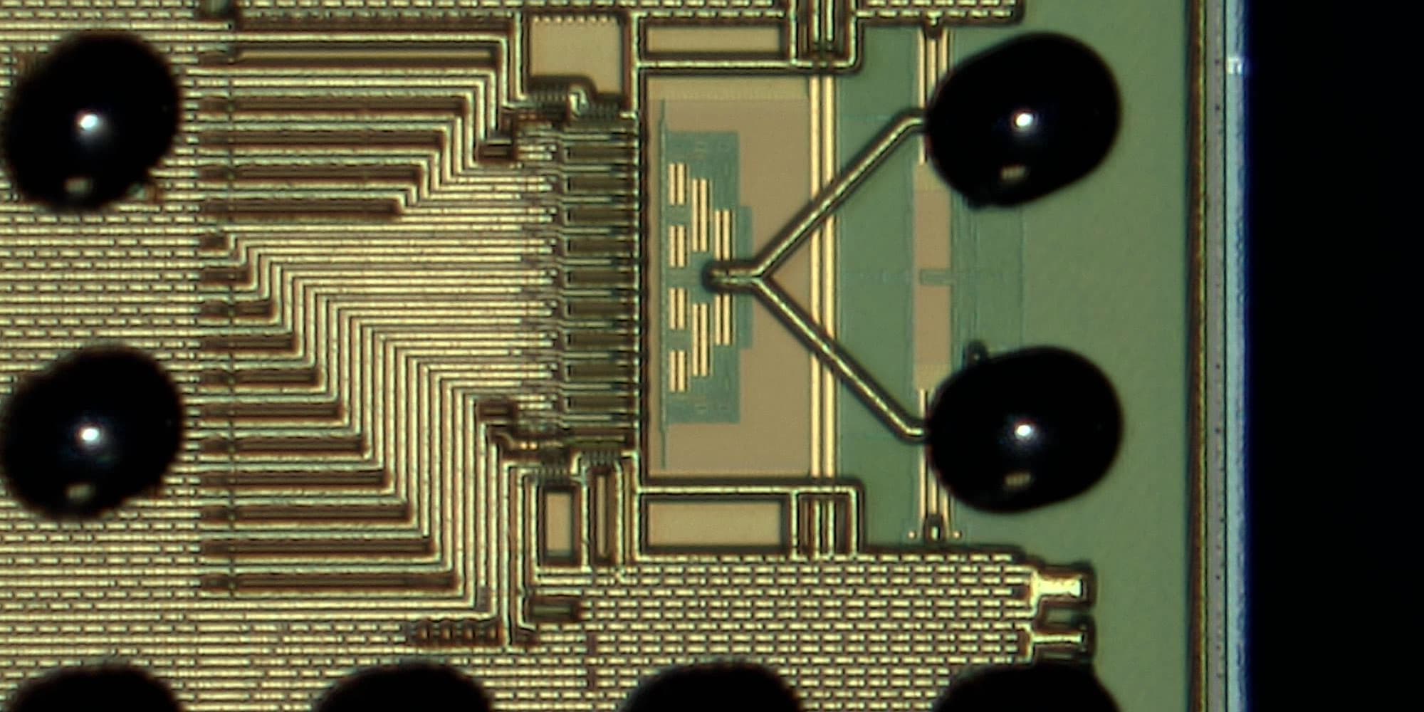
Why 3D integration? Nadine Collaert: “When we go to ever-higher frequencies, the wavelength decreases, and the area of the antenna array scales accordingly. Above 100GHz, however, the antenna pitch gets smaller than the front-end circuit pitch, while the area of the mm-wave radio chip hardly continues scaling. The footprint of the antenna array sets the constraints, but to fit everything underneath the antenna, we will need advanced heterogeneous integration options exploring the 3rd dimension.”
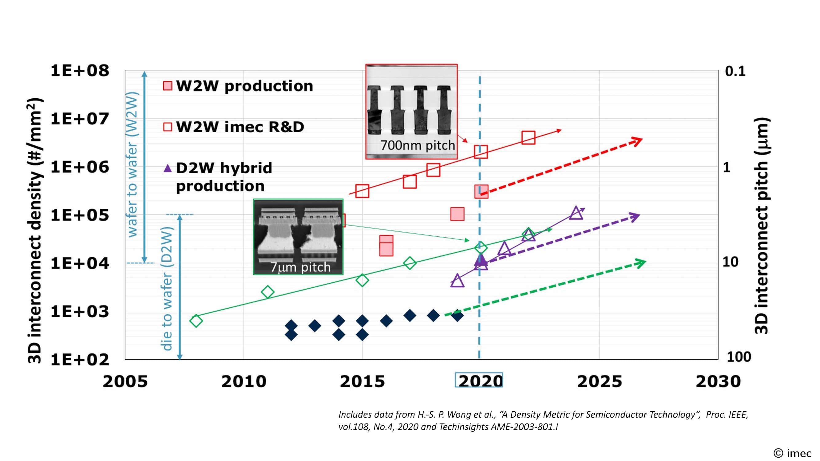
“Over the last decade, tremendous progress has been made in the 3D interconnect landscape. For wafer-level options (wafer-to-wafer, die-to-wafer), there has been an enormous push to reduce the interconnect pitch. In the case of wafer-to-wafer or hybrid bonding, we can achieve pitches below 1µm can and continuously push down further to 500nm and beyond. The same trend to scale the pitch holds for die-to-wafer bonding and die stacking using micro-bumps.”
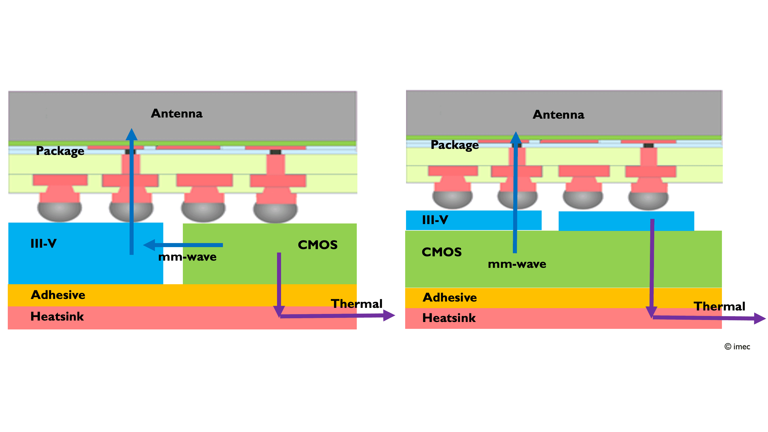
Several challenges are shared between the two integration schemes for >100GHz cases. First, they both rely on having a fine via or micro-bump pitch below 100µm. Second, they should accommodate large numbers of connections for routing (RF, DC, IF, and digital) signals. And finally, both the trace and space dimensions need to be much smaller than 50µm (preferably in the 5-10um range). But there are also differences. In the case of 2/2.5D integration, the III-V sits next to the CMOS chip, enabling better thermal management because both chips can be in direct contact with a heat sink. The disadvantage is that your footprint may need to be relaxed in 1 dimension for some applications, and this architecture only allows for 1D beam steering. 3D integration, on the other hand, allows you to fit all chips and circuits under the antenna and enables 2D beam steering, which directs the signal across a hemisphere. 2D beam steering will be necessary for 5G and beyond applications to minimize penetration losses and increase the reach at the high frequencies needed. The thermal management, finally, is more challenging. And, of course, 3D integration is a more complex approach that comes with its unique processing challenges.
System technology co-optimization leads the way
The choice for which integration and packaging solution ultimately depends on the use case or application. “Because there are so many options available, imec has launched a new STCO (system technology co-optimization) program to guide the technology choices even at the system level. The STCO methodology uses inputs from architecture and application constraints, taking into account signal loss, bandwidth, heat dissipation, mechanical stability, and cost assessment. We will have to consider all these parameters together to design and build the devices for the 6th generation,” concludes Michael Peeters.
Want to know more?
This article was originally published in Microwave Journal.
Authors

Nadine Collaert
Nadine Collaert is program director at imec and responsible for the High-speed analog/RF program. She received an M.S. and Ph.D. degree in electrical engineering from the ESAT Department, KU Leuven, Belgium, in 1995 and 2000, respectively. Since then, she has been involved in the theory, design and technology of FinFET devices, emerging memory devices, transducers for biomedical applications and the heterogeneous integration of new materials with Si.

Michael Peeters
“If you can't explain it simply, you don't understand it well enough.” This quote, attributed to Einstein, Feynman, and others, encapsulates the key element in achieving success in every endeavor in research and development. Whether it pertains to technical or business aspects, this principle drives the three skills that Michael constantly aims to improve: understanding, communicating, and focusing on reducing things to their core.
Currently, Michael Peeters serves as the Vice President and Sector lead of Connected Computing at imec, focussing on creating new approaches to computing, connectivity and their joint architecture, and pushing existing approaches to their utmost performance, to enable continued sustainable growth and the positive impact of computing on society in the coming decade. Previous experiences as CTO for respectively the Wireline and Wireless business lines at what is now Nokia were built on the culture, enthusiasm, and love for technology and science fostered during time as a departement director at Bell Labs, as well as the principles of Free Inquiry instilled by his Alma Mater, the Vrije Universiteit Brussel (VUB).
Throughout their research career, which began with a Ph.D. in Applied Physics and Photonics from the Vrije Universiteit Brussel, Michael has authored more than 100 peer-reviewed publications, numerous white papers, and holds patents in the access and photonics domains. Trained as an electrotechnical engineer, he is a senior member of IEEE and a Fellow of the VUB.
Outside of work, Michael Peeters (imec) balances their quest to discover the perfect lasagna recipe with long-distance running to offset the inherent caloric intake. They accept both (he/him) and (they/them) pronouns.