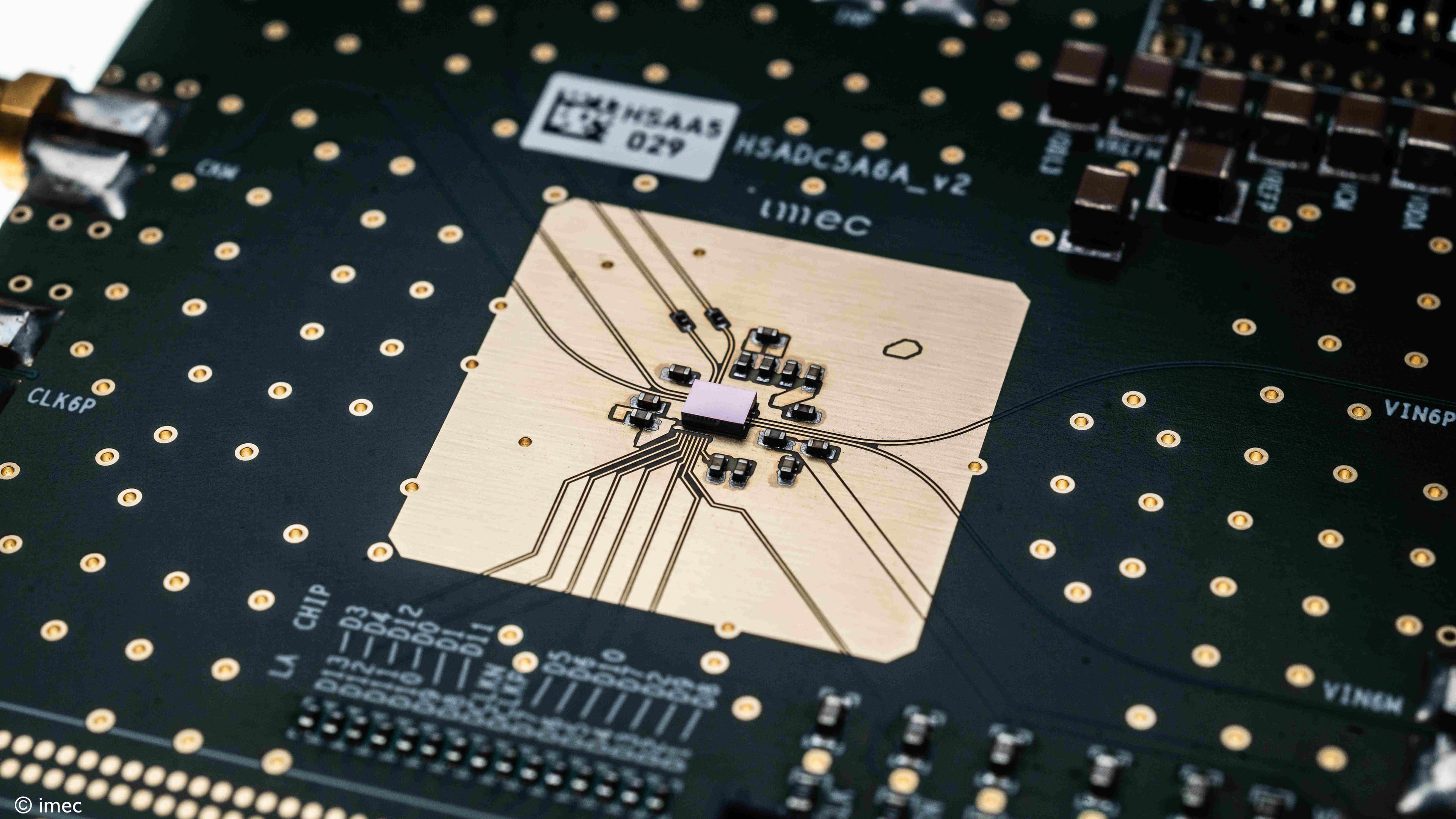
New imec research program pursues the development of scalable and energy-efficient 6G device technology
‘Advanced RF’ initiative wants to make next-gen wireless high-volume applications a commercial reality

LEUVEN (Belgium), November 18, 2020 — Today – at the Japan installment of its ITF 2020 Technology Forum – imec, a world-leading research and innovation hub in nanoelectronics and digital technologies, launched a research program that aims to lay the groundwork for next-gen mobile communications. Dubbed ‘Advanced RF’, imec’s pre-competitive research initiative focuses on creating a roadmap beyond 5G device technology.
One of the paths the imec researchers will explore includes the use of a hybrid III-V/CMOS approach to energy-efficiently and cost-effectively accommodate the very high bandwidths enabled by radio frequencies above 100GHz. Focusing on concrete proof points, imec and its partners will present prototypes that show this approach’s potential. Imec will tap into its broad expertise in the connectivity space to realize the program’s targets – combining its system, circuit and network knowledge with its semiconductor know-how, both in the digital and analog domains.
With bandwidth demands doubling every two years and existing radio spectrum bands getting clogged up, the telecoms industry is looking continuously for novel technologies and approaches to anticipate future mobile communication requirements. Three generations of cellular networks have been introduced since the early 2000s – starting off with the roll-out of 3G, the commercial introduction of 4G in 2009 and today’s deployment of 5G networks. Still, our hunger for bandwidth remains insatiable.
Single-link data rates of 100 Gbit/s, microsecond (µs) latency and new, bandwidth-hungry apps
“There is still some discussion on 6G’s exact characteristics and performance specs, as the actual standardization effort has yet to start,” says Michael Peeters, vice-president of imec’s R&D activities in the connectivity domain. “What is clear, though, is that next-generation wireless networks will largely outsmart their predecessors. Projected features include a 100 Gbit/s single-link throughput, µs latency and a significantly higher energy efficiency – less than 1 nanojoule per bit.”
“We believe this will be crucial to enable concepts such as federated learning between artificial intelligence (AI)-enabled autonomous systems such as self-driving cars. Other use-cases include the deployment of very high-speed, ultra-reliable mobile hot spots in dense urban centers, the support of immersive augmented reality (AR) applications and holography,” he adds.
Tapping into higher radio frequencies in an energy and cost-efficient way
The quest for more bandwidth is inextricably linked with the use of higher radio frequencies: the higher the frequency, the more bandwidth that is available. Hence, while the 5G mobile networks that are on the verge of being deployed will initially operate in the 28 and 39 GHz bands, future mobile networks will resort to frequencies above 100GHz to cater to the world’s growing bandwidth demands. A similar shift to higher frequencies is happening outside of the cellular space as well.
“And that is where we come across one of the main challenges to making affordable solutions a reality – as today’s standard silicon device technology lacks the required transmit power and energy efficiency at higher radio frequencies,” says Nadine Collaert, program director for imec’s analog/RF activities.
“New III-V materials – such as indium phosphide (InP) – might offer a way out, but do not yet lend themselves to be integrated onto a silicon platform. Hence, we will specifically look into hybrid III-V/CMOS approaches. We will investigate how III-V materials can heterogeneously be combined with CMOS technology, how those materials perform in terms of reliability, which degradation mechanisms are at work, etc. Building on those insights, we aim to create mobile device technology that efficiently and cost-effectively operates at 100GHz and beyond,” she says.
The networks that will use these mobile links will likely also need new approaches to the protocol stack from the physical to network layer. The default choice nowadays for high bitrate air interfaces, orthogonal frequency domain multiplexing (OFDM) may no longer be the right choice. More directional beams at higher frequencies can make much more aggressive use of spatial multiplexing. Meshing and even stronger separation of data and control may become needed. Here, we will leverage the expertise we have built e.g. on mmWave channel modelling, dense and short distance meshing, and time sensitive networking.
A prototype that shows the benefits of a hybrid III-V/CMOS approach
“With our Advanced RF program, we aim to extend our impact beyond our pioneering role in the semiconductor space – providing insight and technology across the connectivity ecosystem and not only when it comes to enabling 6G, but also to accommodate the next generation of Wi-Fi communications.”
“It is widely recognized that future mobile networks will have to operate at frequencies above 100GHz to deliver data rates of 100 Gbit/s and more. So far, however, a clear and mature pathway to developing the underlying technology has been lacking,” adds Luc Van den hove, CEO at imec. “With our Advanced RF program, we aim to extend our impact beyond our pioneering role in the semiconductor space – providing insight and technology across the connectivity ecosystem and not only when it comes to enabling 6G, but also to accommodate the next generation of Wi-Fi communications.”
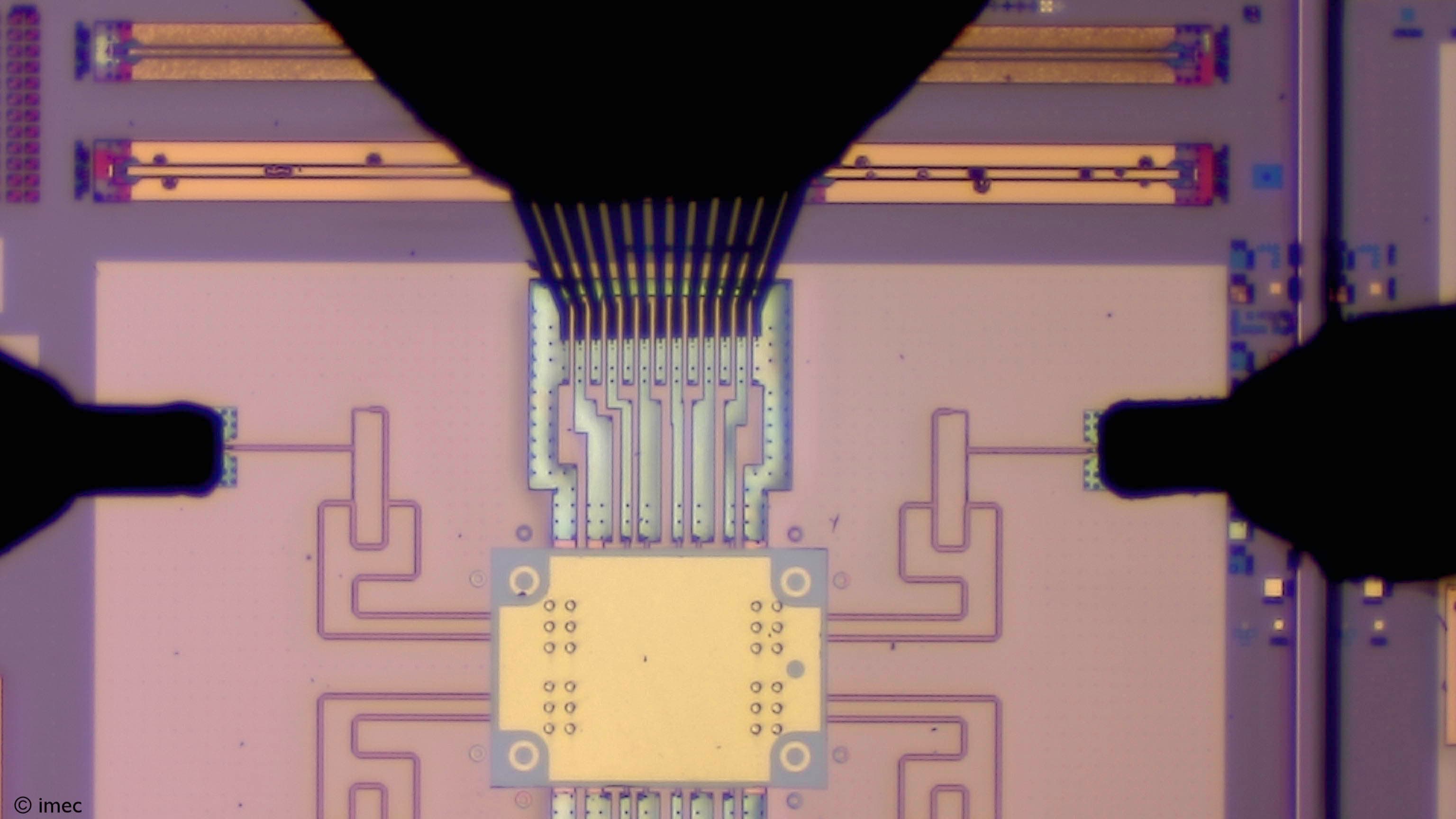
Over the past few years, imec researchers have already conducted quite some research into this topic. One example includes their work in the ECSEL JU ‘Taranto’ project, resulting in the development of an integrated, compact 140GHz radio module that enables single-link data rates up to 80 Gbit/s in an energy-efficient way.
About imec
Imec is a world-leading research and innovation hub in nanoelectronics and digital technologies. The combination of our widely acclaimed leadership in microchip technology and profound software and ICT expertise is what makes us unique. By leveraging our world-class infrastructure and local and global ecosystem of partners across a multitude of industries, we create groundbreaking innovation in application domains such as healthcare, smart cities and mobility, logistics and manufacturing, energy and education.
As a trusted partner for companies, start-ups and universities we bring together more than 4,000 brilliant minds from over 97 nationalities. Imec is headquartered in Leuven, Belgium and has distributed R&D groups at a number of Flemish universities, in the Netherlands, Taiwan, USA, and offices in China, India and Japan. In 2018, imec's revenue (P&L) totaled 583 million euro. Further information on imec can be found at www.imec-int.com.
Imec is a registered trademark for the activities of IMEC International (a legal entity set up under Belgian law as a "stichting van openbaar nut”), imec Belgium (IMEC vzw supported by the Government of Flanders), imec the Netherlands (Stichting IMEC Nederland, part of Holst Centre which is supported by the Dutch Government), imec Taiwan (IMEC Taiwan Co.), imec China (IMEC Microelectronics (Shanghai) Co. Ltd.), imec India (Imec India Private Limited) and imec Florida (IMEC USA nanoelectronics design center).
Discover more

Imec unlocks system-level III-V chiplet integration on Si-CMOS by advancing its 300mm RF silicon interposer platform with high-density MIMCAPs, passive modeling, and laser-assisted bonding
Read more

Imec achieves record-breaking RF GaN-on-Si transistor performance for high-efficiency 6G power amplifiers
Read more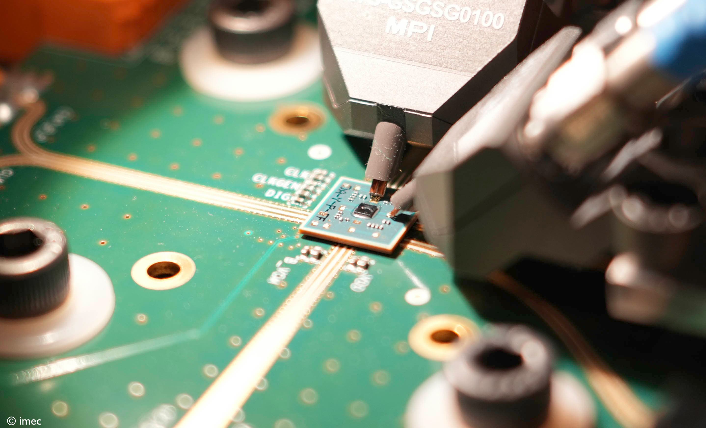
Imec presents 150 GSa/s Digital-to-Analog Converter (DAC) achieving 300 Gb/s data transmission
Read more
Imec and Ghent University present a fully-integrated, single-chip microwave photonics system for compact and versatile signal processing
Read more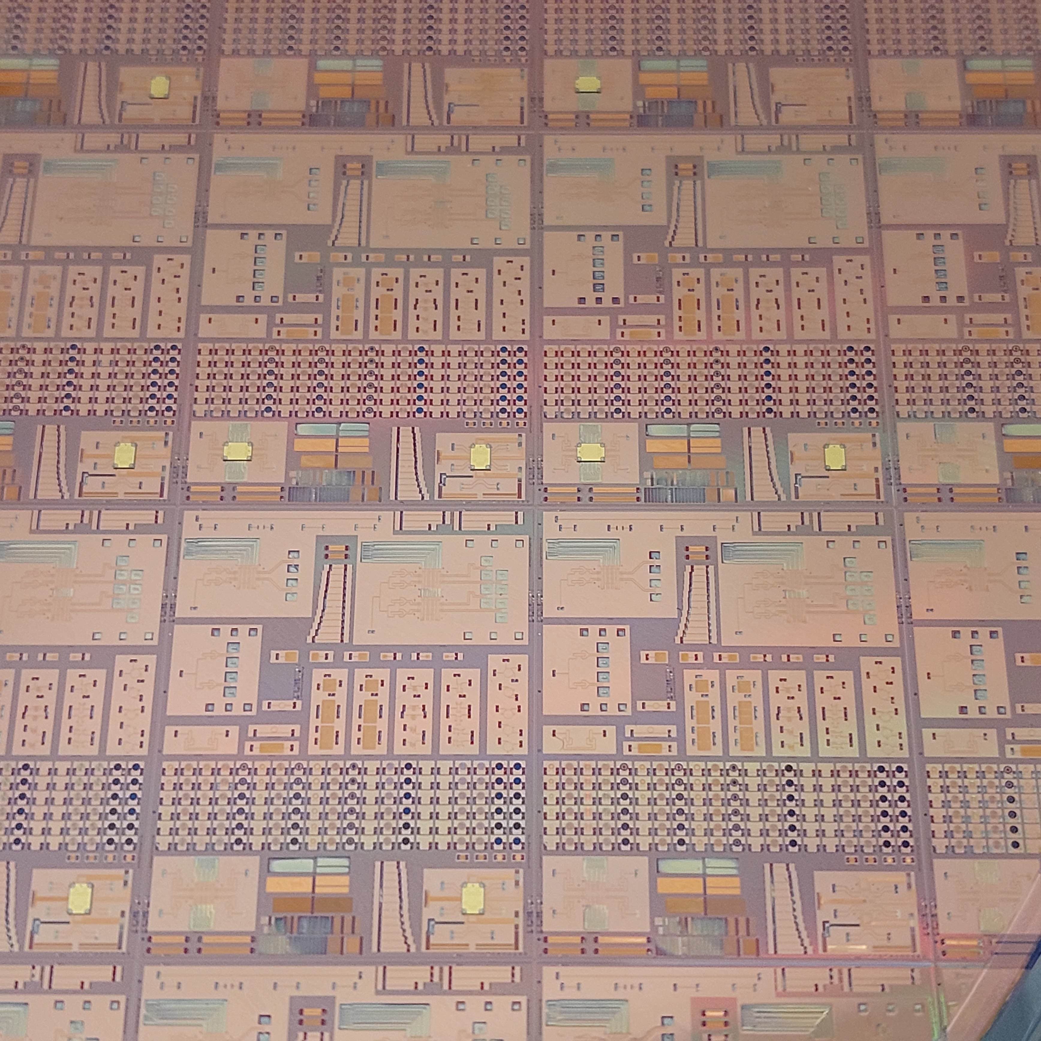
300mm RF silicon interposer platform for chiplet-based heterogeneous integration demonstrates record-low insertion loss at frequencies up to 325GHz
Read more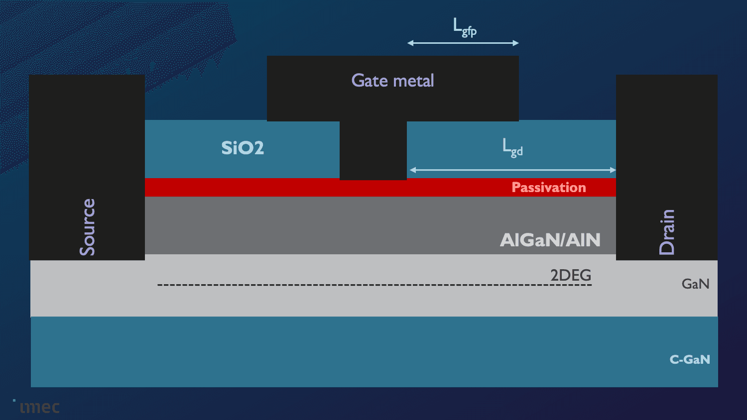
Imec achieves seamless InP Chiplet integration on 300mm RF Silicon Interposer with excellent performance at 140GHz
Read more