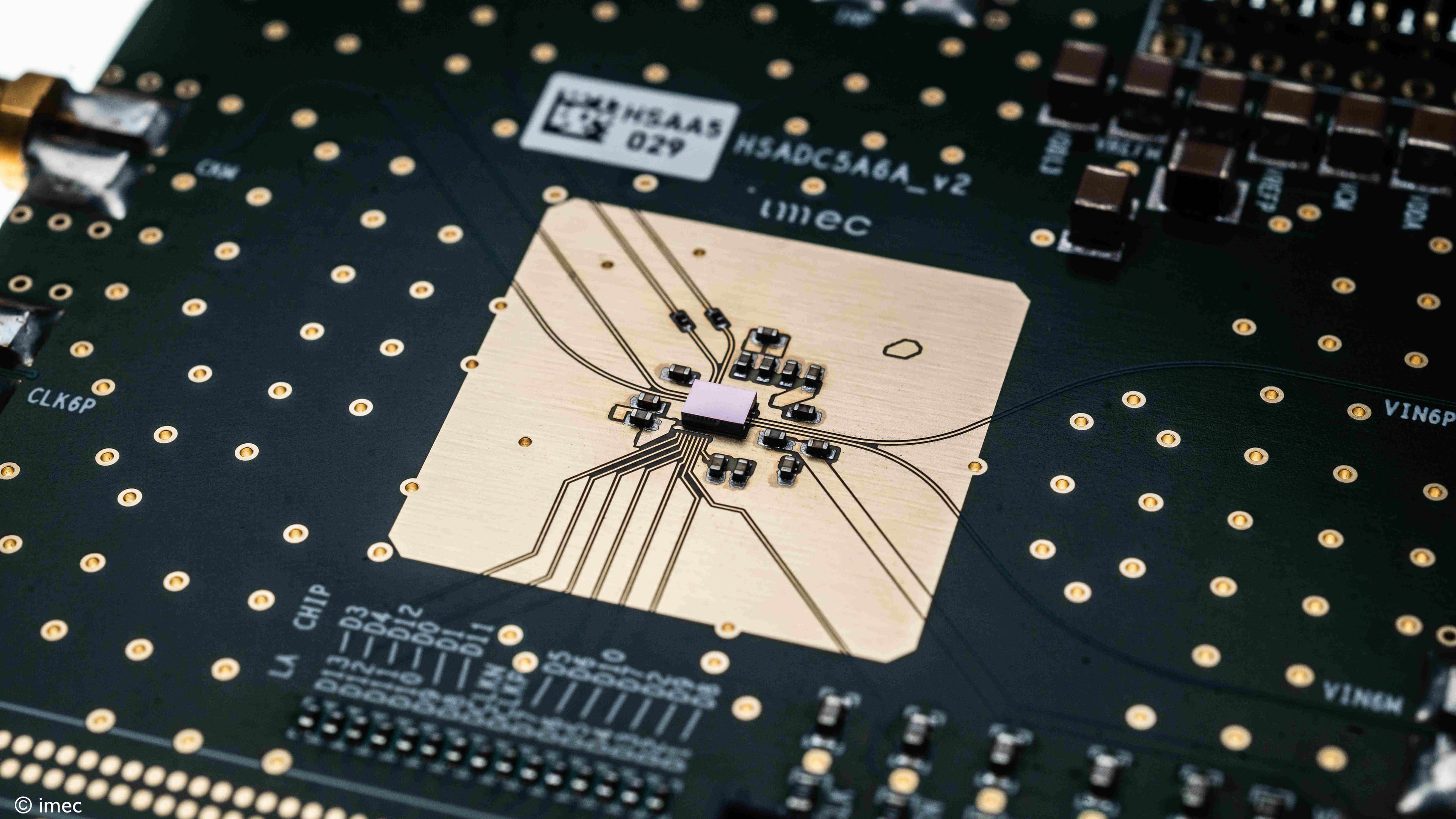
Imec demonstrates GaN-on-Si MISHEMTs with excellent performance for 5G-advanced base station and mobile device applications
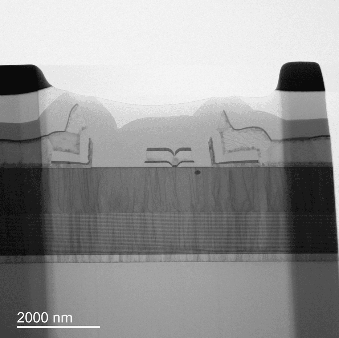
LEUVEN (Belgium), December 12, 2023— This week, at the 2023 International Electron Devices Meeting (IEEE IEDM 2023), imec, a world-leading research and innovation hub in nanoelectronics and digital technologies, presents aluminum-nitride/gallium-nitride (AlN/GaN) metal-insulator-semiconductor high-electron mobility transistors (MISHEMTs) on 200mm Si with high output power and energy efficiency while operating at 28GHz. With these results, imec's GaN-on-Si MISHEMT technology outperforms other GaN MISHEMT device technology in terms of performance, while the adoption of the Si substrate provides a major cost advantage for industrial manufacturing.
Gallium-nitride (GaN) based (MIS)HEMTs are widely explored for 5G-advanced high-capacity wireless communication applications, the next evolutionary step in 5G technology. Due to their outstanding material properties, GaN-based devices offer superior performance over CMOS devices and gallium-arsenide (GaAs) HEMTs in terms of output power and energy efficiency. Industry is looking at two different RF use cases: (1) mobile devices where GaN (MIS)HEMTs are used in power amplifier circuits operating at relatively low voltages (i.e., VDD below 10V); and base stations where VDD voltages are higher (above 20V). For the latter case, GaN-on-silicon-carbide (SiC) devices offer the largest potential, but SiC substrates are expensive and small in size. The ability to integrate GaN HEMTs on Si offers a tremendous cost advantage and potential for technology upscaling, but the performance of GaN-on-Si based (MIS)HEMTs lags behind.
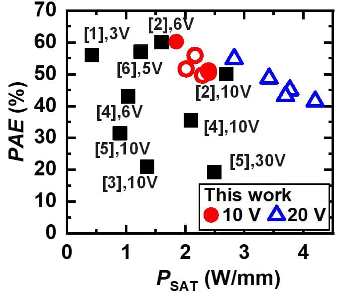
“The challenge is in achieving a high operating frequency (derived from the fT and fmax at small-signal conditions) while at the same time delivering a high output power with sufficient efficiency (derived from the devices large-signal performance),” explains Nadine Collaert, imec fellow and program director advanced RF at imec. “While most GaN devices are HEMTs, in this experimental study, we focused on GaN-on-Si MISHEMTs with AlN barriers as a crucial step towards addressing the demand for both high-power d-mode devices for infrastructure as well as low-voltage e-mode devices required in mobile handsets. These GaN MISHEMT devices, featuring a relaxed gate length of 100nm, demonstrate exceptional performance across various metrics. Specifically, for low-voltage (up to 10V) applications, these devices achieved a saturated output power (PSAT) of 2.2W/mm (26.8dBm) and a power added efficiency (PAE) of 55.5% at 28GHz, positioning our technology better than comparable HEMT/MISHEMTs out there. These results underscore the potential of our technology as a strong foundation for next-generation 5G applications.”
Also, for base stations (20V applications), excellent large-signal performance at 28GHz is demonstrated with a PSAT of 2.8W/mm (27.5dBm) and PAE of 54.8%. “Our AlN/GaN MISHEMTs are still d-mode devices,” adds Nadine Collaert. “But we know the path towards e-mode devices, through further device stack engineering.”
Underlying the performance improvement is a comprehensive study of the impact of the thickness scaling of the AlN and Si3N4 layers, which are used as stop barrier layer, and also gate dielectric, respectively. Ultrathin stacks, for example, enable a high operating frequency, but come at the expense of trapping-induced current collapse and device breakdown in large-signal conditions. A broader study of on-state breakdown of GaN HEMTs, also shown at IEDM, reveals the mechanism behind these reliability issues. “These fundamental studies give us a modelling platform to further optimize the design of our GaN-based material stack for specific use cases,” adds Nadine Collaert.
About imec
Imec is a world-leading research and innovation center in nanoelectronics and digital technologies. Imec leverages its state-of-the-art R&D infrastructure and its team of more than 5,500 employees and top researchers, for R&D in advanced semiconductor and system scaling, silicon photonics, artificial intelligence, beyond 5G communications and sensing technologies, and in application domains such as health and life sciences, mobility, industry 4.0, agrofood, smart cities, sustainable energy, education, … Imec unites world-industry leaders across the semiconductor value chain, Flanders-based and international tech, pharma, medical and ICT companies, start-ups, and academia and knowledge centers. Imec is headquartered in Leuven (Belgium), and has research sites across Belgium, in the Netherlands and the USA, and representation in 3 continents. In 2022, imec's revenue (P&L) totaled 846 million euro.
Further information on imec can be found at www.imec-int.com.
Imec is a registered trademark for the activities of imec International (IMEC International, a legal entity set up under Belgian law as a “stichting van openbaar nut”), imec Belgium (IMEC vzw supported by the Flemish Government), imec the Netherlands (Stichting IMEC Nederland), imec Taiwan (IMEC Taiwan Co.), imec China (IMEC Microelectronics (Shanghai) Co. Ltd.), imec India (IMEC India Private Limited), imec San Francisco (IMEC Inc.) and imec Florida (IMEC USA Nanoelectronics Design Center Inc.).
Discover more

Imec unlocks system-level III-V chiplet integration on Si-CMOS by advancing its 300mm RF silicon interposer platform with high-density MIMCAPs, passive modeling, and laser-assisted bonding
Read more

Imec achieves record-breaking RF GaN-on-Si transistor performance for high-efficiency 6G power amplifiers
Read more
Imec presents 150 GSa/s Digital-to-Analog Converter (DAC) achieving 300 Gb/s data transmission
Read more
Imec and Ghent University present a fully-integrated, single-chip microwave photonics system for compact and versatile signal processing
Read more
300mm RF silicon interposer platform for chiplet-based heterogeneous integration demonstrates record-low insertion loss at frequencies up to 325GHz
Read more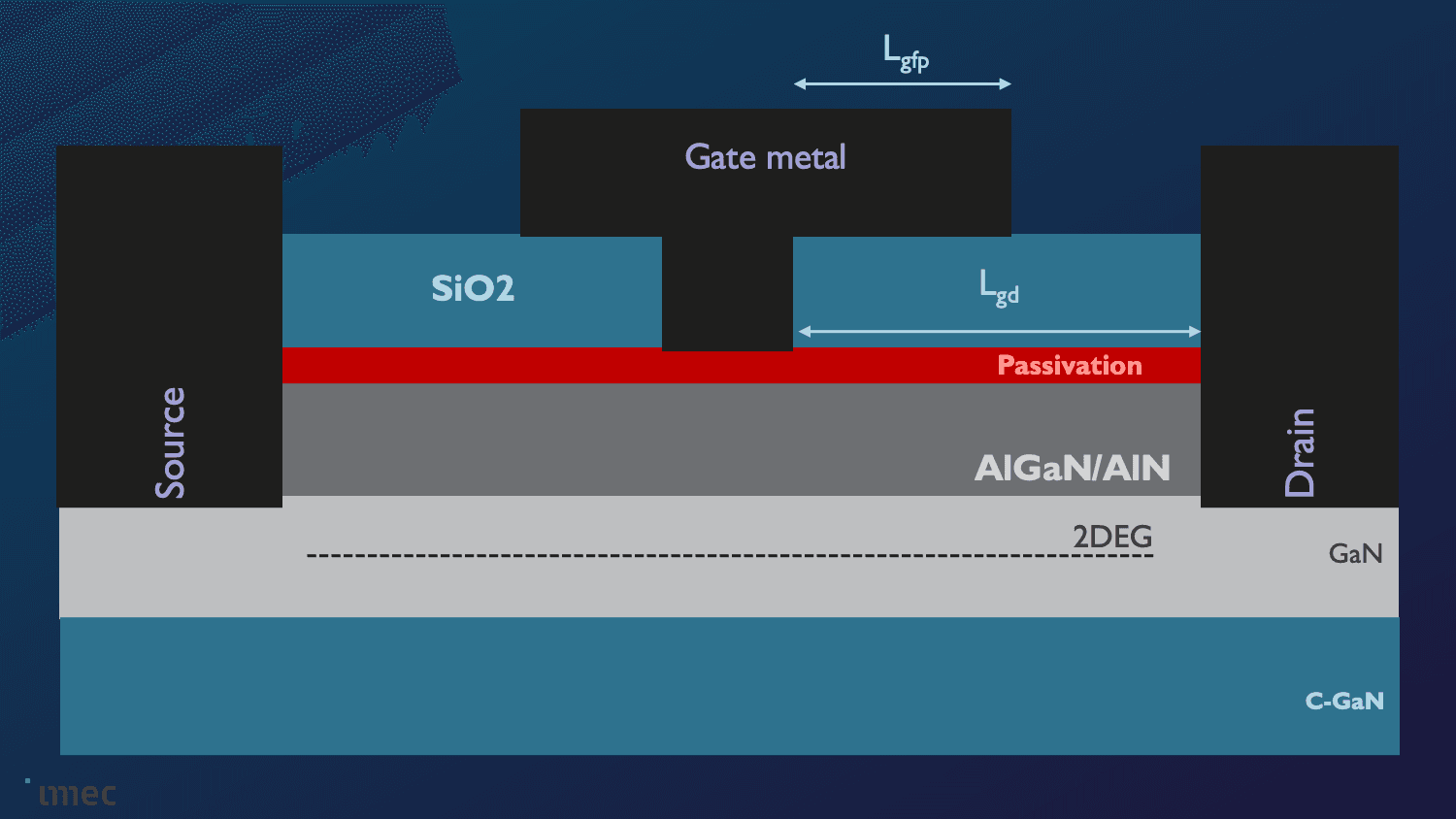
Imec achieves seamless InP Chiplet integration on 300mm RF Silicon Interposer with excellent performance at 140GHz
Read more