Infrared and 3D sensing technology
From AR/VR to autonomous driving and face recognition: tomorrow’s consumer applications need affordable imaging technologies that transcend the visible spectrum. That’s why imec’s Pixel Technology Explore activity is looking into innovative routes towards low-cost, high-resolution infrared sensors and 3D imaging.

CMOS technology has made visible imaging compact, low-power and affordable. Just about every smartphone now harbors a digital camera that’s capable of professional photography.
But the needs of the market are changing. Applications such as augmented reality and face recognition, autonomous driving and food scanning require a shift from imaging to sensing – from taking a picture to acquiring information.
The challenge is to bring these new imaging applications within reach of the consumer technology market, by lowering their cost without compromising their resolution. This is the goal of imec’s Pixel Technology Explore research activities, which break new ground in NIR/SWIR sensing and 3D imaging.
Imec intends to develop technologies for companies with a roadmap in innovative image sensors, cameras and smart imaging applications.
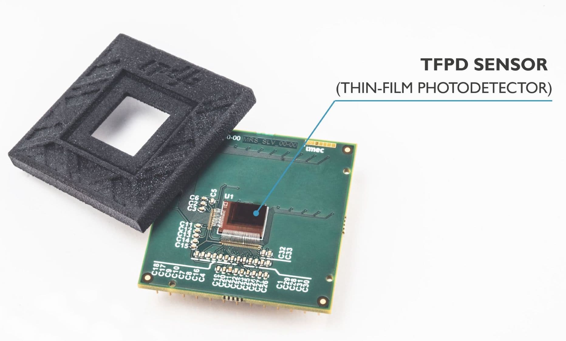
Near-infrared (NIR) and short-wave infrared (SWIR) sensing technology
The sensitivity range of silicon-based sensors is fundamentally limited to below 1100 nm. That’s why infrared imaging has been dominated by III-V detectors that are flip-chip-bonded to silicon readout circuits. This both drives up the costs and limits the pixel pitch and resolution.
The Pixel Technology Explore activity is looking at two methods for cost-effective uncooled IR detection:
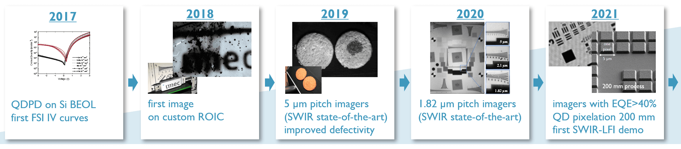
- thin film on silicon – Materials such as organic and colloidal quantum dots offer low-cost synthesis, compatibility with a variety of substrates and processing feasibility on a large area. This article gives you an in-depth view.
- hybrid infrared imagers – Both III-V hetero-epitaxy on silicon and III-V material transfer on silicon are compatible with processing in a silicon wafer fab and reduce the manufacturing costs of IR sensors.
In-depth article: pioneering advances in semiconductor design for sensing light beyond the visible
2024 press release: Imec and partners unveil SWIR sensor with lead-free quantum dot photodiodes
Watch this demonstration of SWIR imaging. The imec QDPD camera captures the image through the silicon wafer:
Silicon-based pixels for 3D sensing
Making use of the third dimension is another way of extending picture content beyond visible photography. For 3D sensing, imec is exploring these research avenues:
- IR laser dot projection – This is addressed by the research topics above that look into uncooled IR detection.
- Continuous Wave (indirect) Time-of-Flight (CW-ToF) – This also relies on an NIR laser pulse but measures the reflected light phase difference within each pixel to get access to distance.
- Direct Time-of-Flight (D-ToF) – This combines an NIR laser pulse with high speed Single Photon Avalanche Diodes (SPAD) that measure the time for a photon to travel between the laser source and the imager.
Want to become our partner in developing new infrared sensing technologies?
As our partner in the Pixel Technology Explore activity, you’re provided with:
- TCAD/optical simulations and pixel architectures
- device demonstrators with analog readout
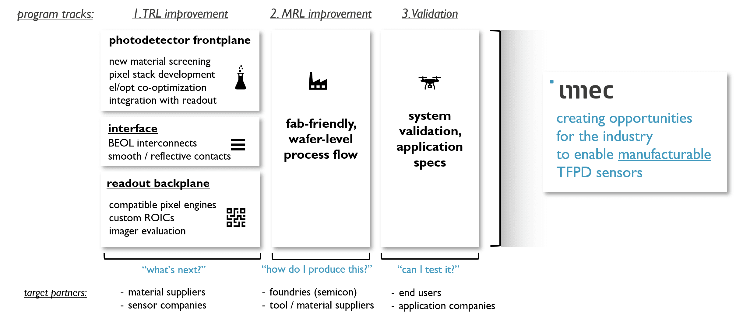
- process integration at die and wafer level (200/300 mm)
- PCM testing and pixel characterization (PTC, QE, MTF, ...)
- material characterization (TEM, SEM, AFM, ...)
We can also assist you with the development of prototypes. Here, you can take advantage of imec’s unique combination of expertise regarding imaging R&D – from material research all the way up to camera integration.
Imec not only helps you to address technological challenges. Thanks to our thorough knowledge of the industry, we function as your full-fledged strategic partner – right down to venturing support.
Click the button below to get in touch.
Links
- Leaflet: Thin-film infrared imagers
- Press release: Imec Presents a Thin-Film Short-Wave-InfraRed Image Sensor with Sub-2µm Pixel Pitch
- Press release: Imec reports monolithic thin-film image sensor for the SWIR range with record pixel density
- Article: SWIR cost cut: Imec achieves 1.82µm pixels
- Article: Building low-cost infrared sensors with sub-micron films (registration required)
- Article: Make smartphones and autonomous vehicles see the impossible
- Blogpost: Imec PbS QD photodiodes for CMOS integration
- Blogpost: Imec Quantum Dot Sensor
Go from R&D to development and manufacturing with IC-Link
Are you ready to accelerate your path from concept to production?
Publications
Z. Lin et al. "VIS-SWIR wideband lens-free imaging", SPIE BOIS, (2021)
External linkJ. LEE et al. "Imaging in Short-Wave Infrared with 1.82 μm Pixel Pitch Quantum Dot Image Sensor", IEEE International Electron Devices Meeting (IEDM), (2020)
External linkJ. Lee et a. "Image sensors for low cost infrared imaging and 3D sensing", SPIE Defense + Commercial Sensing, (2020)
External linkE. Georgitzikis et al. “Integration of PbS quantum dot photodiodes on silicon for NIR imaging”, IEEE Sensors Journal 2019
External linkP.E. Malinowski et al. “NIR/SWIR monolithic image sensors enabled by thin-film photodiode stacks”, SPIE Optics+Photonics 2019, San Diego, US (11th-15th Aug 2019)
External linkY. Li et al. “Beyond BEOL Interconnect Wafer Level Monolithic Near-Infrared/Infrared Thin Film Photo Diode Image Sensor Integration”, IEEE IITC/MAM 2019, Brussels, BE (3rd-6th Jun 2019)
External linkE. Georgitzikis et al. “Optimization of Charge Carrier Extraction in Colloidal Quantum Dots Short‐Wave Infrared Photodiodes through Optical Engineering”, Advanced Functional Materials, Vol. 28 (42), (2018)
External linkF. Verstraeten et al. “Near-infrared organic photodetectors based on bay-annulated indigo showing broadband absorption and high detectivities up to 1.1 μm”, Journal of Materials Chemistry C, (2018)
External linkP.E. Malinowski et al. “Thin-Film Quantum Dot Photodiode for Monolithic Infrared Image Sensors”, MDPI Sensors 17(12), 2867, (2017)
External linkP.E. Malinowski et al. “Organic photodetectors with active layer patterned by lithography”, 2015 IEEE SENSORS, (2015)
External linkE. Georgitzikis et al. “Organic- and QD-based image sensors integrated on 0.13 μm CMOS ROIC for high resolution, multispectral infrared imaging”, IISW 2019, (2019)
External linkE. Georgitzikis et al. “NIR Sensors Based on Photolithographically Patterned PbS QD Photodiodes for CMOS Integration”, IEEE Sensors, (2018)
External linkP.E. Malinowski et al. “Monolithic Near Infrared Image Sensors Enabled by Quantum Dot Photodetector”, IISW, (2017)
External linkE. Georgitzikis et al. “Determining charge carrier extraction in lead sulfide quantum dot near infrared photodetectors”, SPIE Nanoscience + Engineering, (2017)
External linkP. E. Malinowski et al. “Organic photodetectors with active layer patterned by lithography”, IEEE Sensors, (2015)
External linkP. E. Malinowski et al. “Photolithographic patterning of organic photodetectors with a non-fluorinated photoresist system”, Organic Electronics 15 (10), (2014)
External link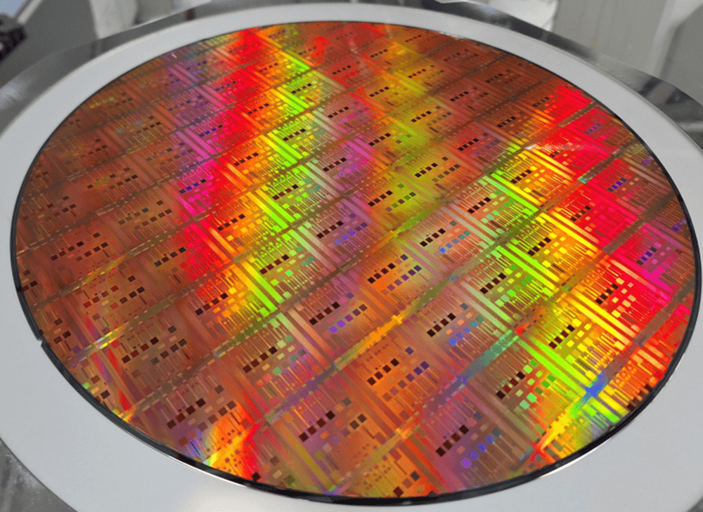
Imec successfully integrates colloidal quantum dot photodiodes (QDPDs) on metasurfaces developed on 300mm CMOS wafers
Pioneering approach makes compact, cost-effective, high-resolution multispectral shortwave infrared (SWIR) sensors accessible, enabling broad application in security, agriculture, automotive, aerospace, and more.
Read more
White paper: monolithic microsystems
Learn how to elevate your application to new heights with advanced functionalities on top of CMOS.
Read more
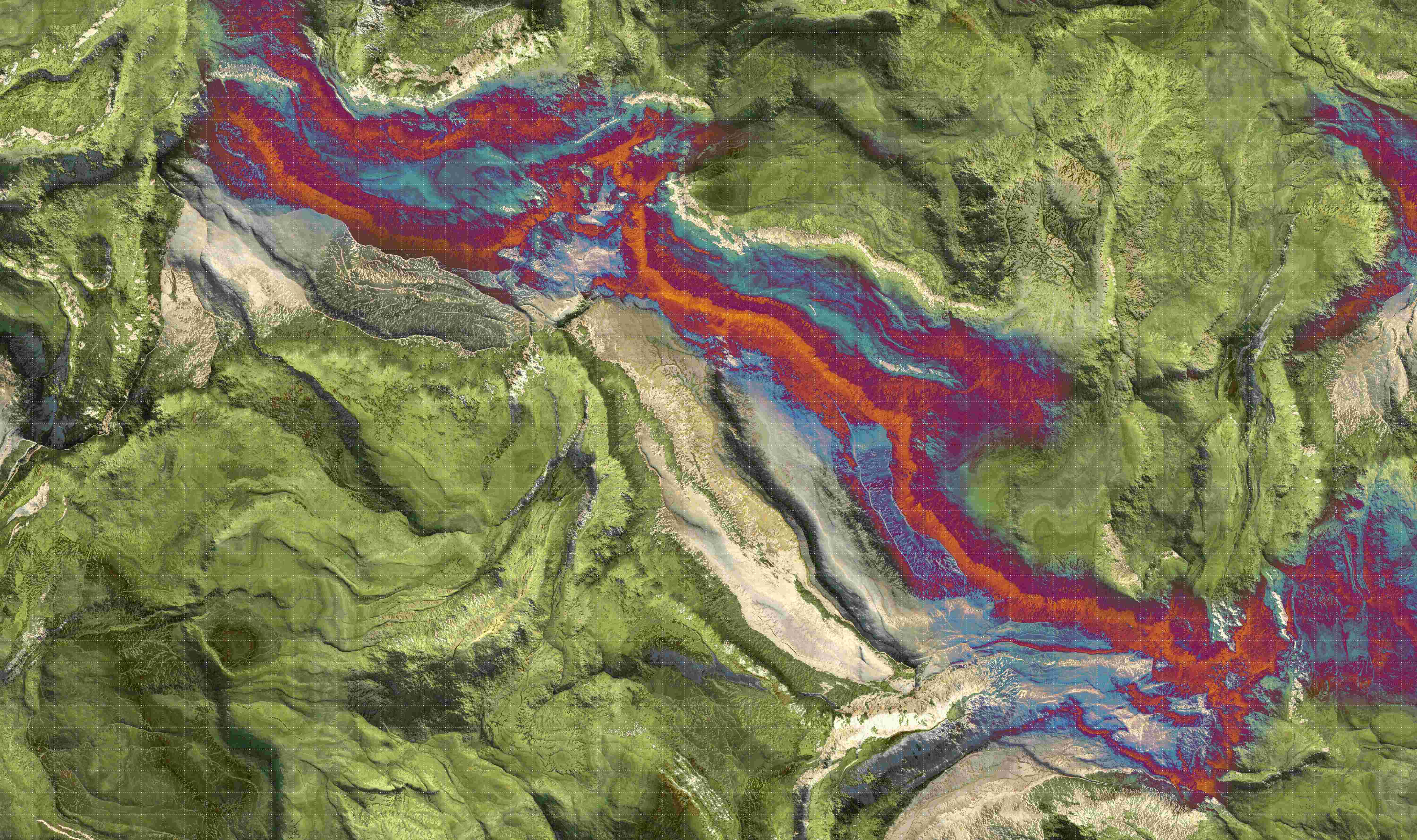
Imec hyperspectral sensor aboard newly launched earth-observation satellite
The IPERLITE mission is designed to demonstrate next-generation hyperspectral imaging technology in space. At the core is a hyperspectral sensor developed by imec.
Read more