Imec Presents a Thin-Film Short-Wave-InfraRed Image Sensor with Sub-2µm Pixel Pitch
The monolithic integration of the thin-film photodetector with CMOS readout circuitry offers a path to high-throughput wafer-level manufacturing
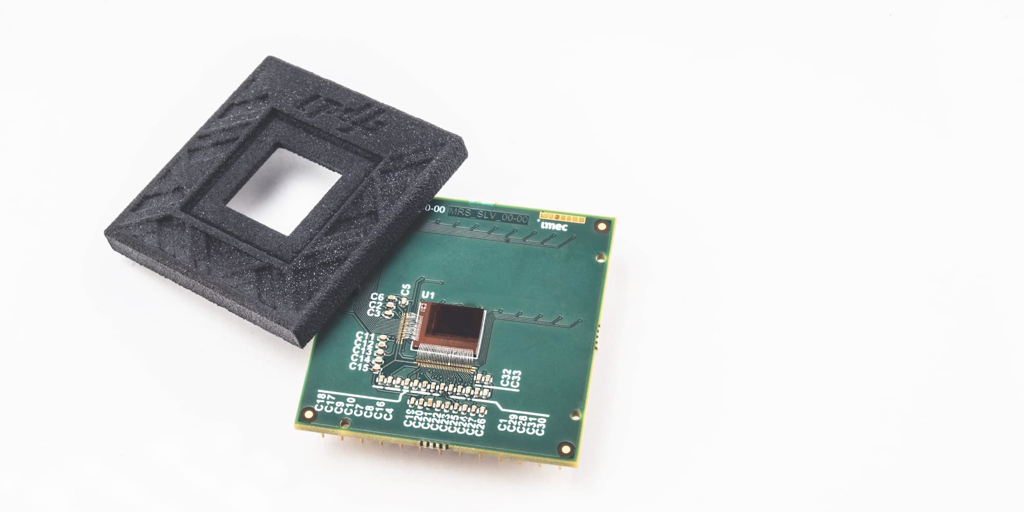
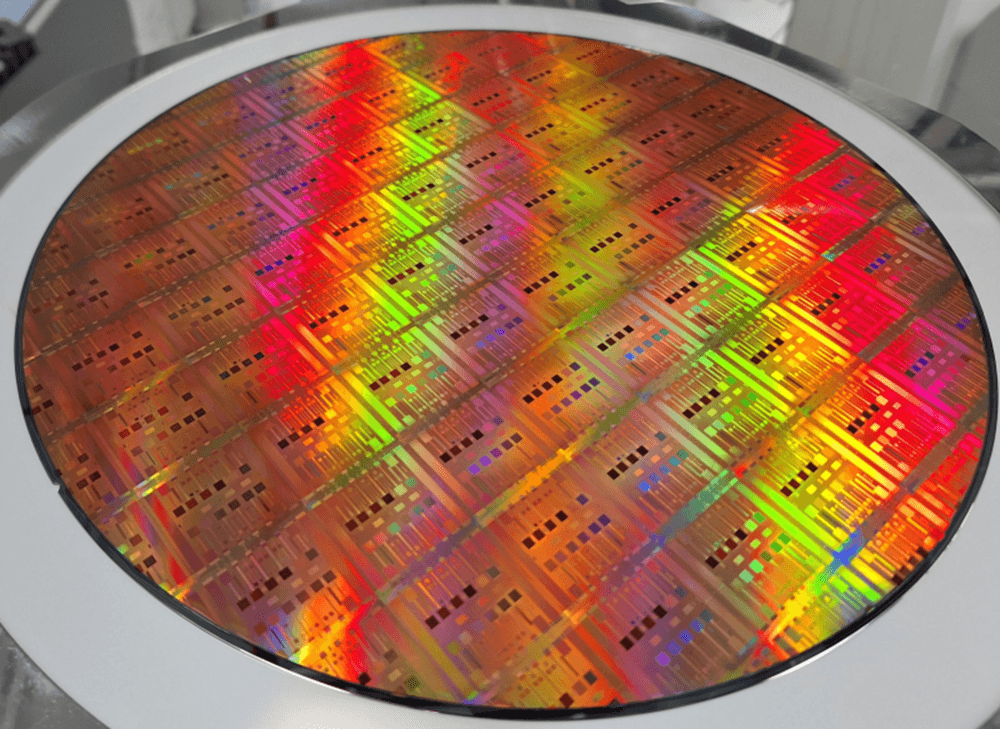
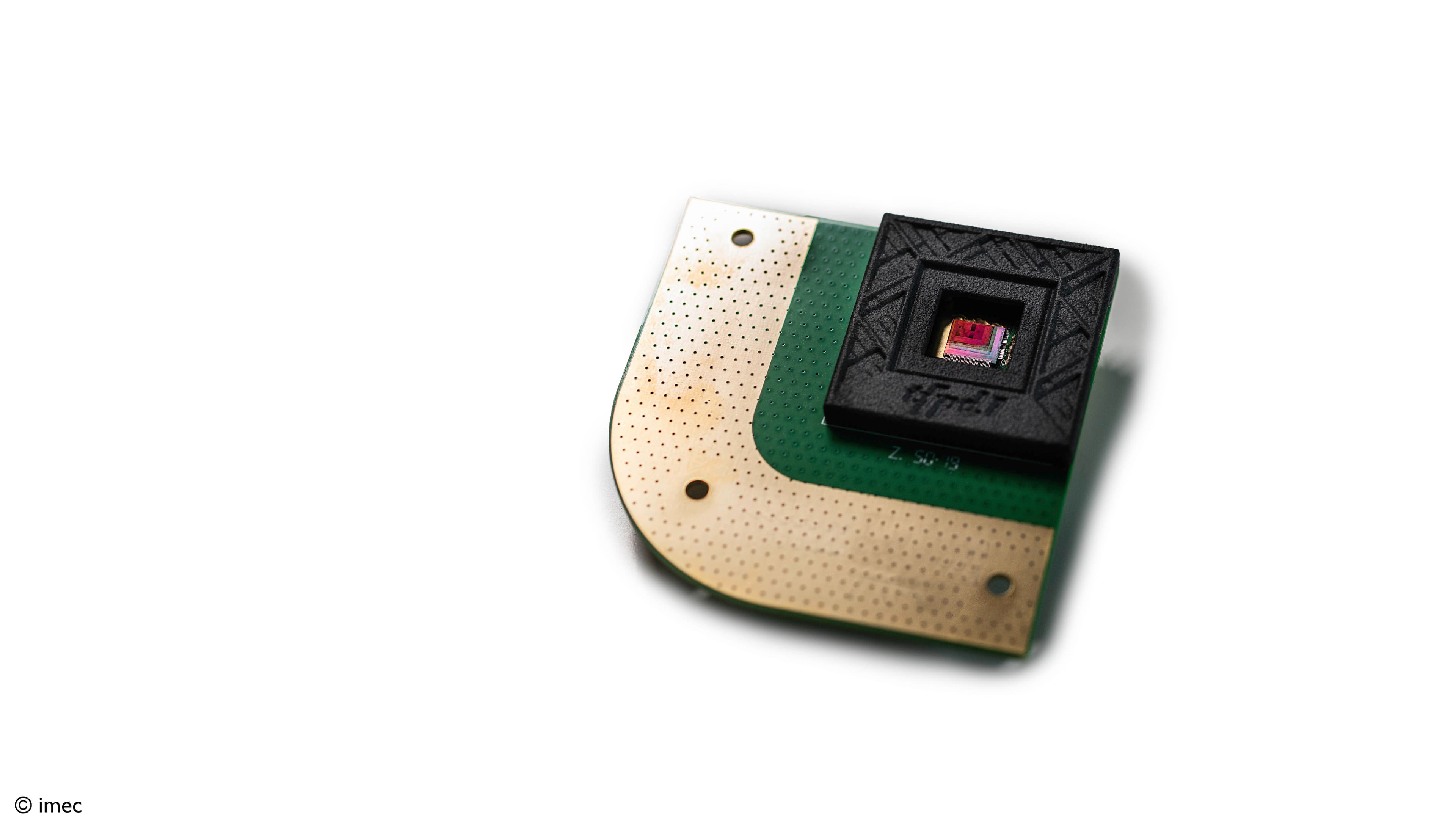
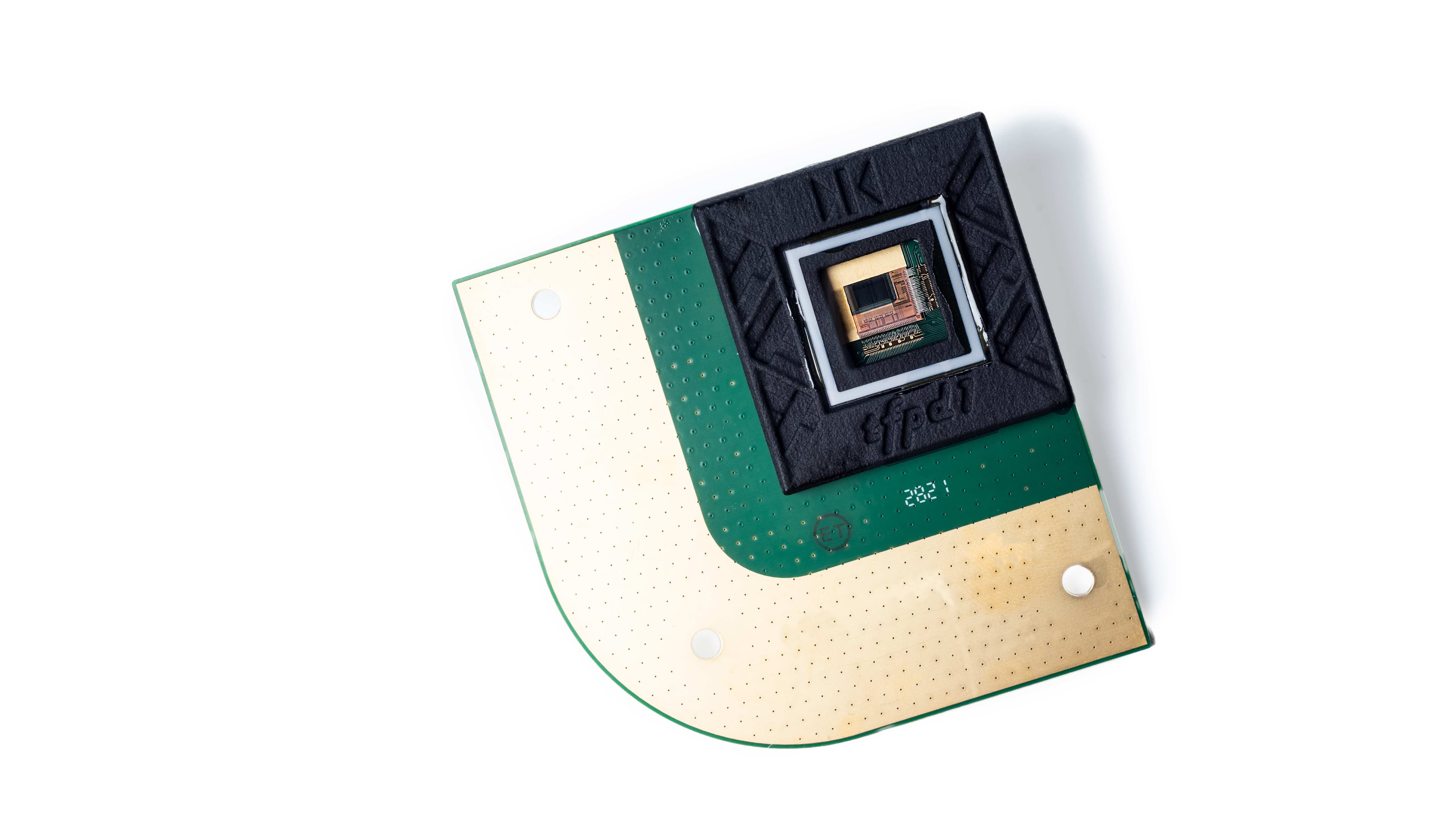
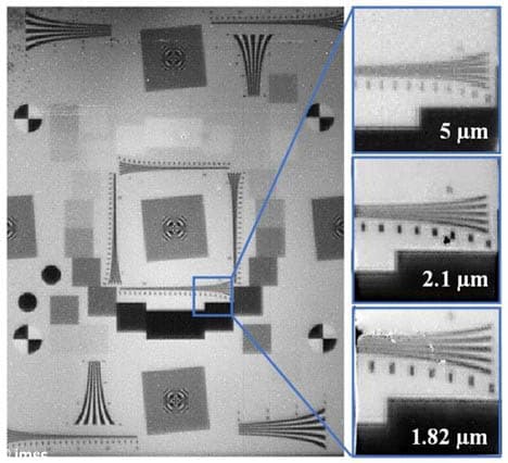
LEUVEN (Belgium), 9 December, 2020 — Imec, a world-leading research and innovation hub in nanoelectronics and digital technologies, presents a prototype high-resolution short-wave-infrared (SWIR) image sensor with record small pixel pitch of 1.82 µm. It is based on a thin-film photodetector that is monolithically integrated on a custom Si-CMOS readout circuit. A fab-compatible process flow paves the way to high-throughput, wafer-level manufacturing. The presented technology largely exceeds the capabilities of today’s InGaAs-based SWIR imagers in terms of pixel pitch and resolution, with disruptive cost and form factor potential. New applications are enabled even in cost-sensitive domains, such as in industrial machine vision, smart agriculture, automotive, surveillance, life sciences and consumer electronics. Imec will present these results at the 2020 IEEE International Electron Devices Meeting (IEDM) in session 16.
Sensing in the short-wavelength infrared (SWIR) range (with wavelengths from around 1400 nm to above 2000 nm) offers advantages over the visible (VIS) and near-infrared (NIR) range for some applications. SWIR image sensors can, for example, see through smoke or fog, or even through silicon – which is especially relevant for inspection and industrial machine vision applications. To date, SWIR image sensors are produced through a hybrid technology, in which a III-V-based photodetector (usually InGaAs-based) is flip-chip bonded to a silicon readout circuit. These sensors can be made extremely sensitive, but the technology is quite expensive for mass manufacturing and limited in size of pixel and number of pixels – hindering its adoption in markets for which cost, resolution and/or form factor are crucial.
Imec introduces an alternative solution that enables record small sub-2 µm pixel pitch, by monolithically integrating a thin-film photodetector stack with a Si-CMOS readout circuit. The photodetector pixel stack implements a thin absorber layer such as 5.5 nm PbS quantum dots – corresponding to peak absorption at 1400 nm wavelength. The peak absorption wavelength can be tuned by adjusting the nanocrystal size and is extendable to wavelengths even above 2000 nm. At the peak SWIR wavelength, an external quantum efficiency (EQE) of 18% is obtained (and can be upgraded towards 50% with further improvements). The photodetector stack is monolithically integrated with a custom readout circuit, processed in 130 nm CMOS technology. In this readout circuit, the 3-transistor pixel design was optimized for the scaling of pixel size in the accessible 130 nm technology node, resulting in record small pitch of 1.82 µm for the prototype SWIR imager.
“With our compact, high resolution SWIR image sensor technology, we offer our customers a path to affordable low-volume manufacturing within imec’s 200 mm facility."
Pawel Malinowski, imec’s thin-film imagers program manager: “With our compact, high resolution SWIR image sensor technology, we offer our customers a path to affordable low-volume manufacturing within imec’s 200 mm facility. These image sensors can be deployed in industrial machine vision (e.g. photovoltaic panel monitoring), smart agriculture (e.g. inspection and sorting), automotive, surveillance, life sciences (e.g. lens-free imaging) and many more. Due to their small form factor, they can potentially be integrated in small cameras, such as in smartphones or AR/VR glasses – with eye-safe SWIR light sources. Some of exciting future developments include increasing of the EQE (which currently is already at 50% in SWIR on test samples), reducing the sensor noise and introducing multispectral arrays with customized patterning approach.”
The prototype SWIR image sensor was developed in imec’s Pixel Technology Explore research program. In this activity, imec collaborates with material companies, image sensor companies, equipment suppliers and technology integrators to develop accessible innovative and customized CMOS imaging technologies.
About imec
Imec is a world-leading research and innovation hub in nanoelectronics and digital technologies. The combination of our widely acclaimed leadership in microchip technology and profound software and ICT expertise is what makes us unique. By leveraging our world-class infrastructure and local and global ecosystem of partners across a multitude of industries, we create groundbreaking innovation in application domains such as healthcare, smart cities and mobility, logistics and manufacturing, energy and education.
As a trusted partner for companies, start-ups and universities we bring together more than 4,000 brilliant minds from over 97 nationalities. Imec is headquartered in Leuven, Belgium and has distributed R&D groups at a number of Flemish universities, in the Netherlands, Taiwan, USA, and offices in China, India and Japan. In 2018, imec's revenue (P&L) totaled 583 million euro. Further information on imec can be found at www.imec-int.com.
Imec is a registered trademark for the activities of IMEC International (a legal entity set up under Belgian law as a "stichting van openbaar nut”), imec Belgium (IMEC vzw supported by the Government of Flanders), imec the Netherlands (Stichting IMEC Nederland, part of Holst Centre which is supported by the Dutch Government), imec Taiwan (IMEC Taiwan Co.), imec China (IMEC Microelectronics (Shanghai) Co. Ltd.), imec India (Imec India Private Limited) and imec Florida (IMEC USA nanoelectronics design center).