Imec and partners unveil SWIR sensor with lead-free quantum dot photodiodes
The technology marks a crucial step towards environmentally friendly infrared imagers to transform autonomous driving, medical diagnostics and more
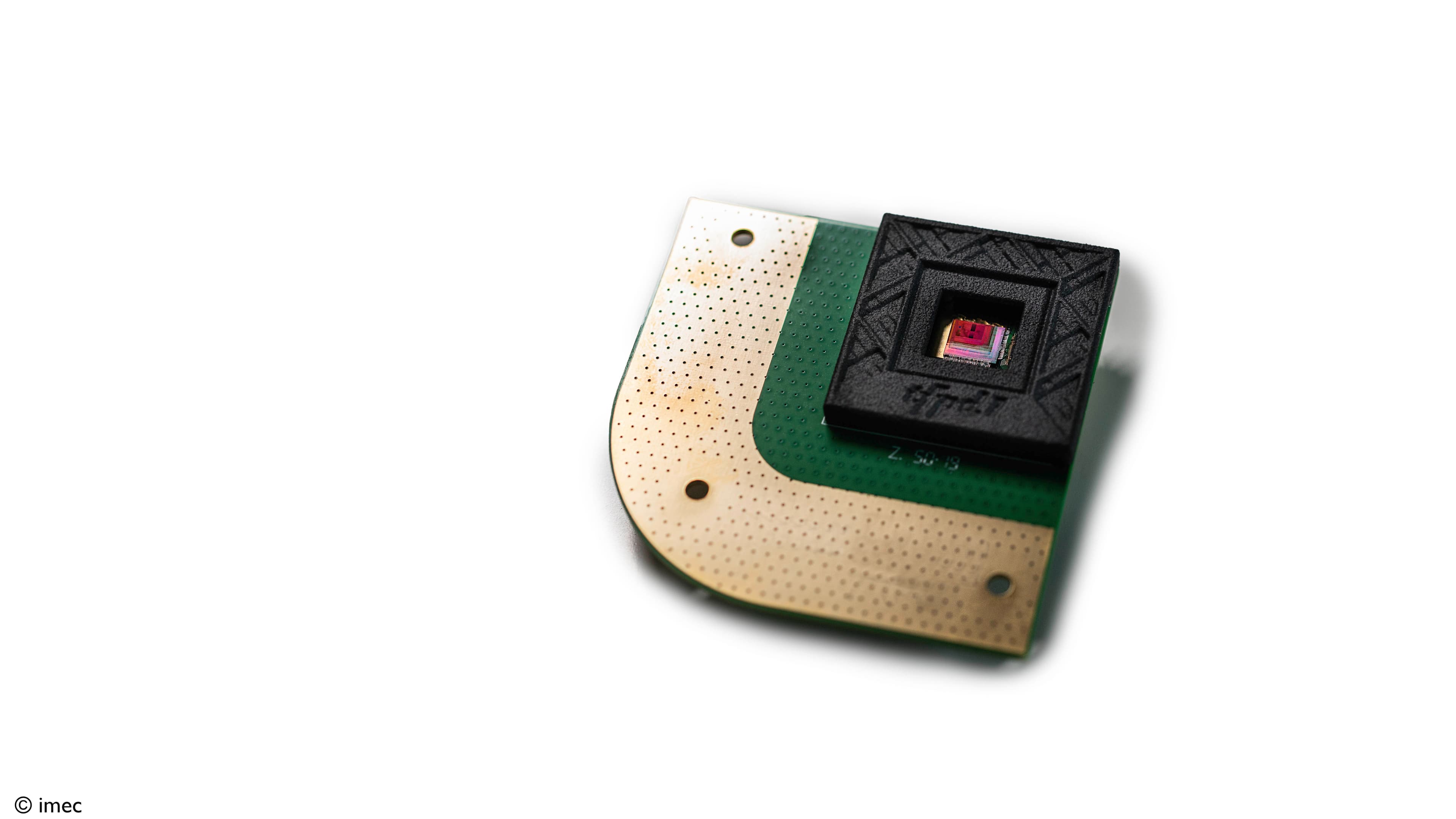
LEUVEN (Belgium), December 16, 2024— This week, at the 2024 IEEE International Electron Devices Meeting (IEDM), imec, a world-leading research and innovation hub in nanoelectronics and digital technologies, and its partners in the Belgian project Q-COMIRSE, present a first of its kind prototype shortwave infrared image sensor with indium arsenide quantum dot photodiodes. The sensor demonstrated successful 1390 nm imaging results, offering an environmentally friendly alternative to first-generation quantum dots that contain lead, which limited their widespread manufacturing. The proof-of-concept is a critical step toward mass-market infrared imaging with low-cost and non-toxic photodiodes.
By detecting wavelengths beyond the visible spectrum, shortwave infrared (SWIR) sensors can provide enhanced contrast and detail, as materials reflect differently in this range. These sensors can distinguish objects that appear identical to the human eye and penetrate through fog or mist, making them invaluable for applications such as face recognition or eye tracking in consumer electronics, and autonomous vehicle navigation. While current versions are costly and limited to high-end applications, wafer-level integration promises broader accessibility.
Quantum dots (QDs) are nanoscale semiconductor particles that can be engineered to emit and absorb light at specific wavelengths. Tuned for SWIR, they offer compact, low-cost absorbers, since integration into CMOS circuits and existing manufacturing processes is possible. However, first-generation QDs often contain toxic heavy metals such as lead and mercury, and the search for alternatives continues.
At 2024 IEDM, imec and its partners within the Q-COMIRSE project (Ghent University, QustomDot BV, ChemStream BV and ams OSRAM) introduced a SWIR image sensor featuring a lead-free quantum dot alternative as absorber; indium arsenide (InAs). The proof-of-concept sensor, tested on both glass and silicon substrates, was the first of its kind to produce successful 1390 nm imaging results. While QDs are considered fragile in nature, careful selection of stack materials resulted in >300 hour air-stability, enabling fab manufacturing compatibility. The pixel architecture can readily be integrated with CMOS technology for image sensing applications, but also allows flat panel display integration.
Pawel Malinowski, imec technology manager and domain lead imaging, emphasized the significance of this breakthrough: "The first generation of QD sensors was crucial for showcasing the possibilities of this flexible platform. We are now working towards a second generation that will serve as a crucial enabler for the masses - aiming at cost-efficient manufacturing in an environmentally friendly way. With major industry players looking into quantum dots, we are committed to further refine this semiconductor technology towards accessible, compact, multifunctional image sensors with new functionalities."
Stefano Guerrieri, Engineering Fellow at ams OSRAM, added: "Replacing lead in colloidal quantum dots with a more environmentally friendly material was our key goal in Q-COMIRSE. Our remarkable development work with Flemish partners imec, Ghent University, QustomDot and ChemStream paves the way toward a low-cost and Pb-free short-wave-infrared technology that, once mature for industrial products, could enable unprecedented applications in robotics, automotive, AR/VR and consumer electronics among others."
This work was performed within the Q-COMIRSE project, funded by SIM-Flanders (HBC.2021.0803), the spearhead cluster for materials in Flanders, Belgium. Consortium partners included imec, Ghent University, QustomDot BV, ChemStream BV and ams OSRAM sensor Belgium.
About imec
Imec is a world-leading research and innovation center in nanoelectronics and digital technologies. Imec leverages its state-of-the-art R&D infrastructure and its team of more than 5,500 employees and top researchers, for R&D in advanced semiconductor and system scaling, silicon photonics, artificial intelligence, beyond 5G communications and sensing technologies, and in application domains such as health and life sciences, mobility, industry 4.0, agrofood, smart cities, sustainable energy, education, … Imec unites world-industry leaders across the semiconductor value chain, Flanders-based and international tech, pharma, medical and ICT companies, start-ups, and academia and knowledge centers. Imec is headquartered in Leuven (Belgium), and has research sites across Belgium, in the Netherlands, the UK and the USA, and representation in 3 continents. In 2023, imec's revenue (P&L) totaled 941 million euro.
Further information on imec can be found at www.imec-int.com.
Imec is a registered trademark for the activities of imec International and its affiliated entities.
Discover more
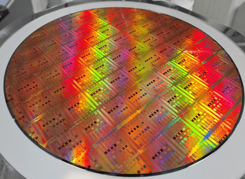
Imec successfully integrates colloidal quantum dot photodiodes (QDPDs) on metasurfaces developed on 300mm CMOS wafers
Read more


From horsepower to high-performance compute: automotive chiplets take the leap towards autonomous edge computing
Read more

Next-gen UWB radio technology to enable radar sensing, data streaming, and advanced ranging applications
Read more