Perovskite LEDs, a thousand times brighter than OLEDs
Imec paves the way for perovskite laser diodes
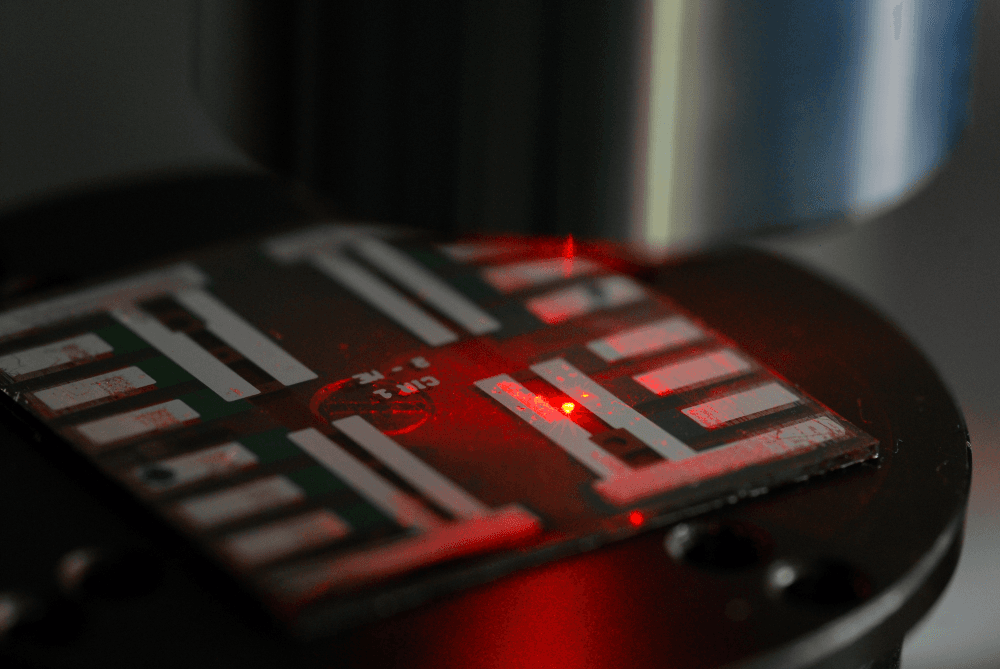
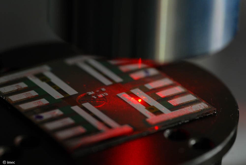
LEUVEN (Belgium), January 4, 2024 —Imec, a world-leading research and innovation hub in nanoelectronics and digital technologies, presents a perovskite LED stack, emitting light a thousand times brighter than state-of-the-art OLEDs. This result, published in this month’s Nature Photonics, is a pivotal milestone towards a perovskite injection laser, promising exciting applications in image projection, environmental sensing, medical diagnostics, and beyond.
Light-emitting diodes (LEDs) have revolutionized modern lighting and sensing technology. From applications in our homes to industry, LEDs are used for all lighting applications, from indoor lighting over TV screens to biomedicine. Widely used organic LEDs (OLEDs) today, for example in smartphone screens, employ organic thin-film materials as a semiconductor. However, their maximum brightness remains limited; just think of trying to read your smartphone screen on a very sunny day.
Meanwhile, perovskites – a class of materials with a specific crystal structure – are proving their worth beyond solar cells. With excellent optoelectrical properties, low-cost processability and efficient charge transport, these materials have emerged in the last ten years as interesting candidates for light emission applications, such as LEDs.
However, while perovskites can withstand very high current densities, laser operation with the emission of high-intensity coherent light has not been reached yet. “In the ULTRA-LUX project, imec showed for the first time a PeLED architecture with low optical losses and pumped these PeLEDs to current densities that support the stimulated emission of light”, explained prof. Paul Heremans, who is an imec senior fellow and principal investigator of the project. “This novel architecture of transport layers, transparent electrodes and perovskite as the semiconductor active material, can operate at electrical current densities tens of thousands of times higher (3 kA cm-2) than conventional OLEDs can.”
“With this architecture, imec enhanced amplified spontaneous emission, with an electrical assist of the conventional optical pumping. By doing so, imec demonstrated that electrical injection contributes 13 percent to the total amount of stimulated emission and thus approaches the threshold to achieve a thin-film injection laser”, stated Robert Gehlhaar, imec project manager. “Reaching this landmark milestone towards high-power thin-film laser diodes is paving the way to exciting new applications of thin-film perovskite lasers.”
The findings are published in Nature Photonics ‘Electrically Assisted Amplified Spontaneous Emission in Perovskite Light Emitting Diodes’. The ULTRA-LUX project has received funding from the European Research Council (ERC) under the European Union’s Horizon 2020 research and innovation program (Grant Agreement No.835133) with an Advanced Grant to Prof. Paul Heremans and is ongoing until September 30th, 2024.
About imec
Imec is a world-leading research and innovation center in nanoelectronics and digital technologies. Imec leverages its state-of-the-art R&D infrastructure and its team of more than 5,500 employees and top researchers, for R&D in advanced semiconductor and system scaling, silicon photonics, artificial intelligence, beyond 5G communications and sensing technologies, and in application domains such as health and life sciences, mobility, industry 4.0, agrofood, smart cities, sustainable energy, education, … Imec unites world-industry leaders across the semiconductor value chain, Flanders-based and international tech, pharma, medical and ICT companies, start-ups, and academia and knowledge centers. Imec is headquartered in Leuven (Belgium), and has research sites across Belgium, in the Netherlands and the USA, and representation in 3 continents. In 2022, imec's revenue (P&L) totaled 846 million euro.
Further information on imec can be found at www.imec-int.com.
Imec is a registered trademark for the activities of imec International (IMEC International, a legal entity set up under Belgian law as a “stichting van openbaar nut”), imec Belgium (IMEC vzw supported by the Flemish Government), imec the Netherlands (Stichting IMEC Nederland), imec Taiwan (IMEC Taiwan Co.), imec India (IMEC India Private Limited), imec San Francisco (IMEC Inc.) and imec Florida (IMEC USA Nanoelectronics Design Center Inc.).
Discover more